MAX7315 Ver la hoja de datos (PDF) - Maxim Integrated
Número de pieza
componentes Descripción
Fabricante
MAX7315
Maxim Integrated

MAX7315 Datasheet PDF : 26 Pages
| |||
8-Port I/O Expander with LED Intensity
Control, Interrupt, and Hot-Insertion Protection
where:
RLED is the resistance of the resistor in series with the
LED (Ω).
VSUPPLY is the supply voltage used to drive the LED (V).
VLED is the forward voltage of the LED (V).
VOL is the output low voltage of the MAX7315 when
sinking ILED (V).
ILED is the desired operating current of the LED (A).
For example, to operate a 2.2V red LED at 14mA from a
5V supply, RLED = (5 - 2.2 - 0.25) / 0.014 = 182Ω.
Driving Load Currents Higher than 50mA
The MAX7315 can be used to drive loads drawing more
than 50mA, like relays and high-current white LEDs, by
paralleling outputs. Use at least one output per 50mA of
load current; for example, a 5V 330mW relay draws
66mA and needs two paralleled outputs to drive it.
Ensure that the paralleled outputs chosen are controlled
by the same blink phase register, i.e., select outputs
from the P0 through P7 range. This way, the paralleled
outputs are turned on and off together. Do not use out-
put O8 as part of a load-sharing design. O8 cannot be
switched at the same time as any of the other outputs
because it is controlled by a different register.
The MAX7315 must be protected from the negative
voltage transient generated when switching off induc-
tive loads, such as relays, by connecting a reverse-
biased diode across the inductive load (Figure 18). The
peak current through the diode is the inductive load’s
operating current.
Power-Supply Considerations
The MAX7315 operates with a power-supply voltage of
2V to 3.6V. Bypass the power supply to GND with at
least 0.047µF as close to the device as possible. For
the QFN version, connect the underside exposed pad
to GND.
Chip Information
TRANSISTOR COUNT: 17,611
PROCESS: BiCMOS
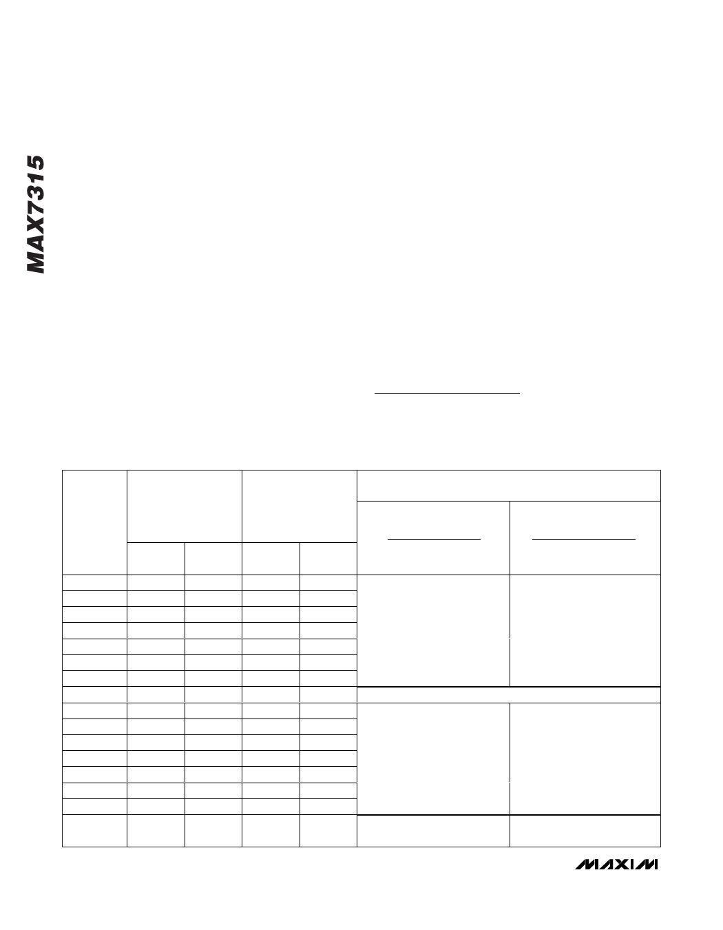
Table 12. PWM Intensity Settings (Blink Enabled)
OUTPUT
(OR
GLOBAL)
INTENSITY
SETTING
0x0
0x1
0x2
0x3
0x4
0x5
0x6
0x7
0x8
0x9
0xA
0xB
0xC
0xD
0xE
0xF
PWM DUTY CYCLE
OUTPUT BLINK
PHASE X
REGISTER BIT = 0
PWM DUTY CYCLE
OUTPUT BLINK
PHASE X
REGISTER BIT = 1
EXAMPLES OF LED BLINK BEHAVIOR
(LED IS ON WHEN OUTPUT IS LOW)
BLINK PHASE 0
REGISTER BIT = 0
BLINK PHASE 0
REGISTER BIT = 1
LOW
TIME
1/16
2/16
3/16
4/16
5/16
6/16
7/16
8/16
9/16
10/16
11/16
12/16
13/16
14/16
15/16
Static low
HIGH
TIME
LOW
TIME
HIGH
TIME
BLINK PHASE 1
REGISTER BIT = 1
BLINK PHASE 1
REGISTER BIT = 0
15/16
15/16
1/16
14/16
14/16
2/16
13/16
12/16
11/16
13/16
12/16
11/16
3/16
Phase 0: LED on at low intensity Phase 0: LED on at high intensity
4/16
Phase 1: LED on at high intensity Phase 1: LED on at low intensity
5/16
10/16
10/16
6/16
9/16
9/16
7/16
8/16
8/16
8/16
Output is half intensity during both blink phases
7/16
7/16
9/16
6/16
6/16
10/16
5/16
5/16
11/16
Phase 0: LED on at high intensity Phase 0: LED on at low intensity
4/16
4/16
12/16
Phase 1: LED on at low intensity Phase 1: LED on at high intensity
3/16
3/16
13/16
2/16
2/16
14/16
1/16
1/16
15/16
Static high Static high Phase 0: LED on continuously Phase 0: LED off continuously
Static low
impedance impedance Phase 1: LED off continuously Phase 1: LED on continuously
20 ______________________________________________________________________________________
Share Link: