MAX7315 Ver la hoja de datos (PDF) - Maxim Integrated
Número de pieza
componentes Descripción
Fabricante
MAX7315
Maxim Integrated

MAX7315 Datasheet PDF : 26 Pages
| |||
8-Port I/O Expander with LED Intensity
Control, Interrupt, and Hot-Insertion Protection
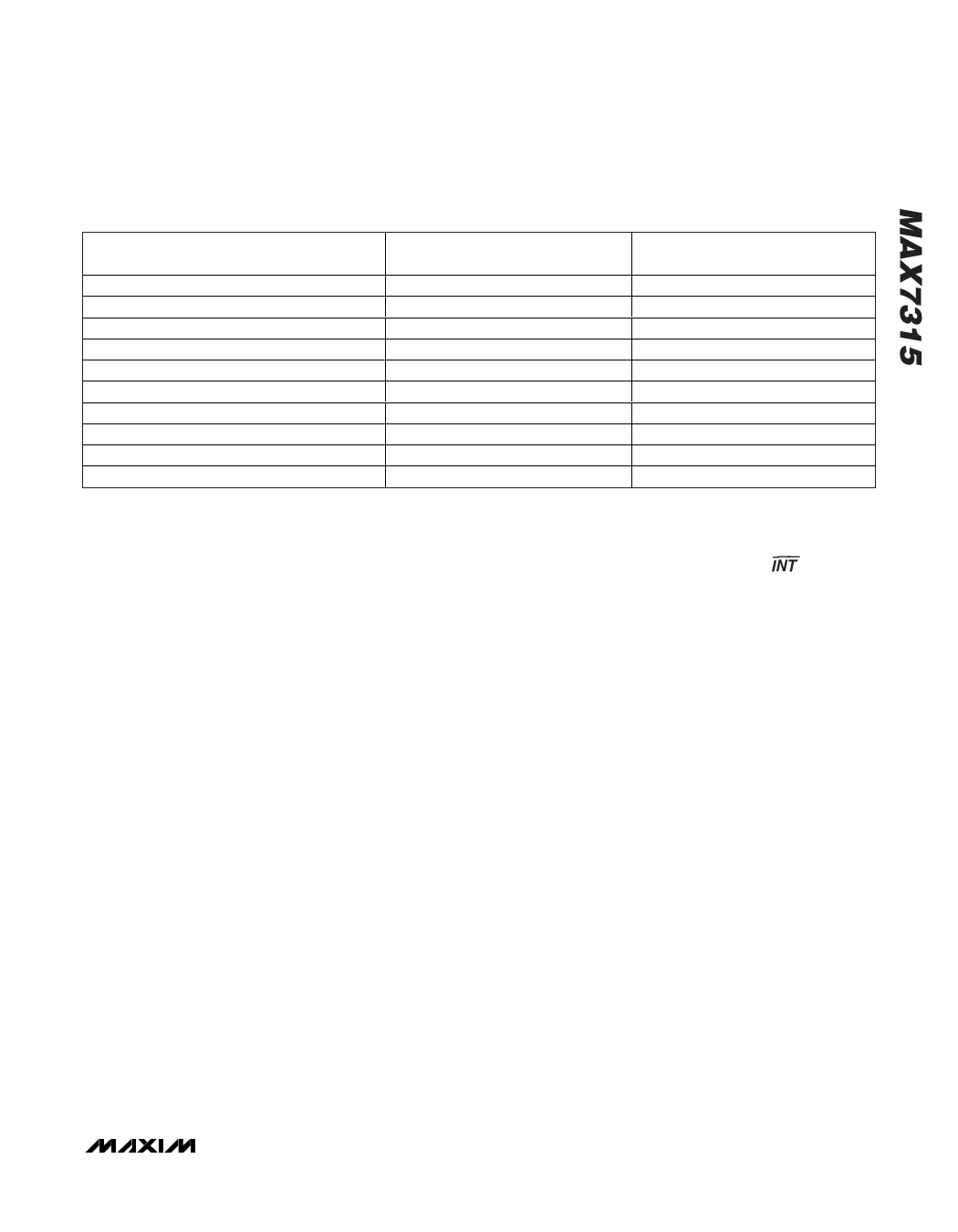
Table 2. Register Address Map
REGISTER
Read input ports
Blink phase 0 outputs
Ports configuration
Blink phase 1 outputs
Master, O8 intensity
Configuration
Outputs intensity P1, P0
Outputs intensity P3, P2
Outputs intensity P5, P4
Outputs intensity P7, P6
ADDRESS CODE
(HEX)
0x00
0x01
0x03
0x09
0x0E
0x0F
0x10
0x11
0x12
0x13
AUTOINCREMENT
ADDRESS
0x00 (no change)
0x01 (no change)
0x03 (no change)
0x09 (no change)
0x0E (no change)
0x0F (no change)
0x11
0x12
0x13
0x10
Ports Configuration
The 8 I/O ports P0 through P7 can be configured to any
combination of inputs and outputs using the ports con-
figuration register (Table 5). The INT/O8 output can also
be configured as an extra general-purpose output
using the configuration register (Table 4).
Input Ports
The input ports register is read only (Table 6). It reflect
the incoming logic levels of the ports, regardless of
whether the port is defined as an input or an output by
the ports configuration register. Reading the input ports
register latches the current-input logic level of the
affected eight ports. A write to the input ports register is
ignored.
Transition Detection
All ports configured as inputs are always monitored for
changes in their logic status. The action of reading the
input ports register or writing to the configuration regis-
ter samples the corresponding 8 port bits’ input condi-
tion (Tables 4, 6). This sample is continuously
compared with the actual input conditions. A detected
change in input condition causes an interrupt condition.
The interrupt is cleared either automatically if the
changed input returns to its original state, or when the
input ports register is read, updating the compared
data (Figure 10). Randomly changing a port from an
output to an input may cause a false interrupt to occur if
the state of the input does not match the content of the
input ports register. The interrupt status is available as
the interrupt flag INT in the configuration register (Table
4).
The input status of all ports is sampled immediately
after power-up as part of the MAX7315’s internal initial-
ization, so if all the ports are pulled to valid logic levels
at that time an interrupt does not occur at power-up.
INT/O8 Output
The INT/O8 output pin can be configured as either the
INT output that reflects the interrupt flag logic state or as
a general-purpose output O8. When used as a general-
purpose output, the INT/O8 pin has the same blink and
PWM intensity control capabilities as the other ports.
Set the interrupt enable I bit in the configuration register
to configure INT/O8 as the INT output (Table 4). Clear
interrupt enable to configure INT/O8 as the O8. O8
logic state is set by the 2 bits O1 and O0 in the configu-
ration register. O8 follows the rules for blinking selected
by the blink enable flag E in the configuration register. If
blinking is disabled, then interrupt output control O0
alone sets the logic state of the INT/O8 pin. If blinking is
enabled, then both interrupt output controls O0 and O1
set the logic state of the INT/O8 pin according to the
blink phase. PWM intensity control for O8 is set by the 4
global intensity bits in the master, O8 intensity register
(Table 13).
Blink Mode
In blink mode, the output ports can be flipped between
using either the blink phase 0 register or the blink phase
1 register. Flip control is by software control (the blink flip
flag B in the configuration register) (Table 4). If hardware
flip control is needed, consider the MAX7316, which
includes a BLINK input, as well as software control.
The blink function can be used for LED effects by pro-
gramming different display patterns in the two sets of
______________________________________________________________________________________ 13
Share Link: