MAX7300 Ver la hoja de datos (PDF) - Maxim Integrated
Número de pieza
componentes Descripción
Fabricante
MAX7300 Datasheet PDF : 20 Pages
| |||
2-Wire-Interfaced, 2.5V to 5.5V, 20-Port or
28-Port I/O Expander
TIMING CHARACTERISTICS (Figure 2) (continued)
(VV+ = 2.5V to 5.5V, TA = TMIN to TMAX, unless otherwise noted.) (Note 1)
Note 1: All parameters tested at TA = +25°C. Specifications over temperature are guaranteed by design.
Note 2: Guaranteed by design.
Note 3: A master device must provide a hold time of at least 300ns for the SDA signal (referred to VIL of the SCL signal) in order to
bridge the undefined region of SCL’s falling edge.
Note 4: Cb = total capacitance of one bus line in pF. tR and tF measured between 0.3V+ and 0.7V+.
Note 5: ISINK ≤ 6mA. Cb = total capacitance of one bus line in pF. tR and tF measured between 0.3V+ and 0.7V+.
Note 6: Input filters on the SDA and SCL inputs suppress noise spikes less than 50ns.
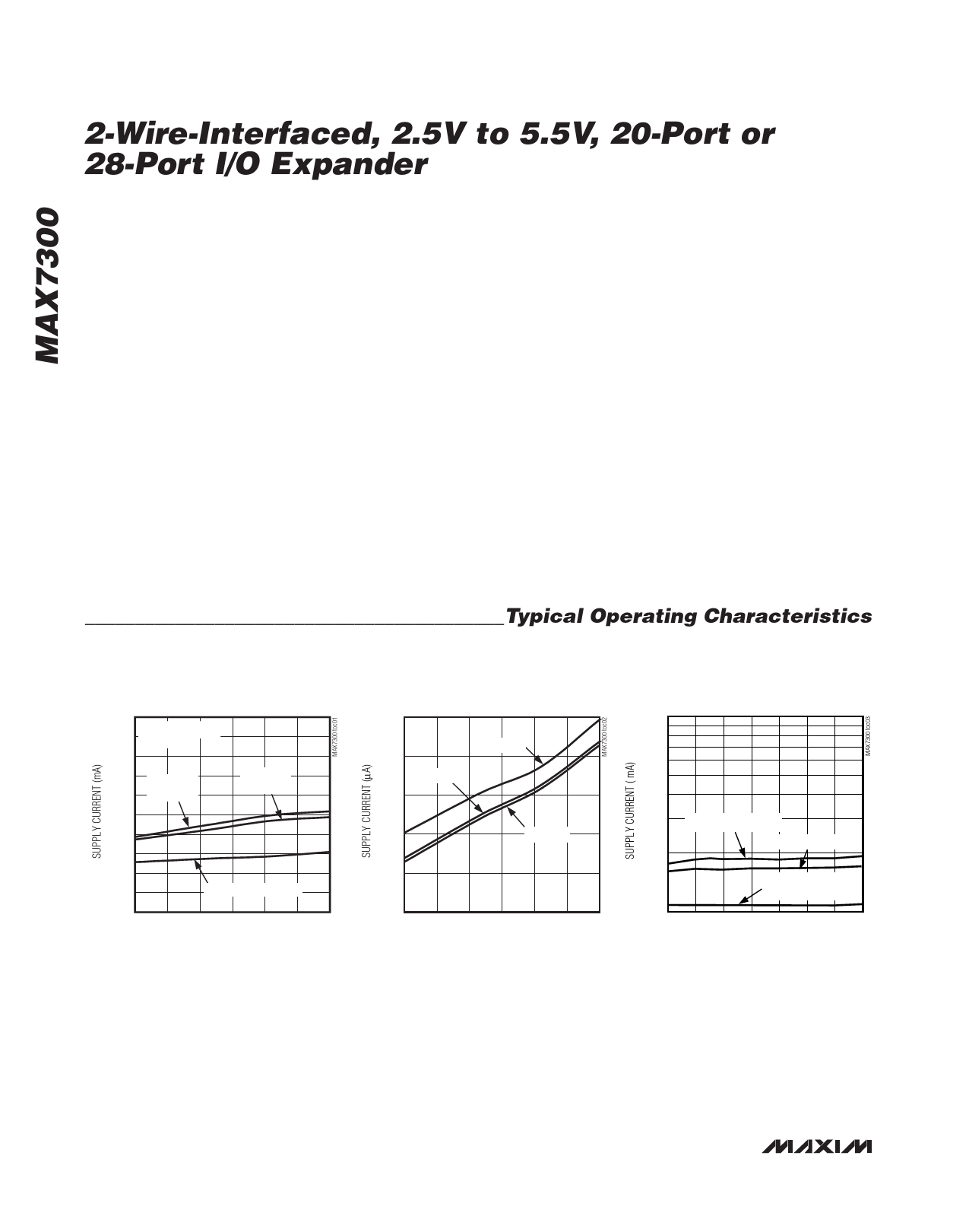
__________________________________________Typical Operating Characteristics
(RISET = 39kΩ, TA = +25°C, unless otherwise noted.)
OPERATING SUPPLY CURRENT
vs. TEMPERATURE
0.40
0.36
VV+ = 2.5V TO 5.5V
NO LOAD
0.32
0.28 ALL PORTS
0.24 OUTPUT (1)
ALL PORTS
OUTPUT (0)
0.20
0.16
0.12
0.08
0.04
ALL PORTS INPUT HIGH
0
-40.0 -12.5 15.0 42.5 70.0
TEMPERATURE (°C)
97.5 125.0
SHUTDOWN SUPPLY CURRENT
vs. TEMPERATURE
8
VV+ = 5.5V
7
VV+ = 3.3V
6
5
VV+ = 2.5V
4
3
-40.0 -12.5
15.0 42.5 70.0
TEMPERATURE (°C)
97.5 125.0
OPERATING SUPPLY CURRENT vs. V+
(OUTPUTS UNLOADED)
1
ALL PORTS OUTPUT (1)
ALL PORTS OUTPUT (0)
ALL PORTS INPUT
(PULLUPS DISABLED)
0.1
2.0 2.5 3.0 3.5 4.0 4.5 5.0 5.5
V+ (V)
4 _______________________________________________________________________________________
Share Link: 