MAX3656(2010) Ver la hoja de datos (PDF) - Maxim Integrated
Número de pieza
componentes Descripción
Fabricante
MAX3656 Datasheet PDF : 15 Pages
| |||
155Mbps to 2.5Gbps Burst-Mode
Laser Driver
Programming the APC Loop
When using the MAX3656’s APC feature, program the
average optical power by adjusting the APCSET resis-
tor. To select this resistor, determine the desired moni-
tor current to be maintained over temperature and
lifetime. See the IMD vs. RAPCSET graph in the Typical
Operating Characteristics and select the value of
RAPCSET that corresponds to the required current.
Setting the LONGB Input Pin
Set the LONGB pin according to Table 2 to optimize
APC loop operation.
Interfacing with Laser Diodes
The laser modulation current output OUT+ is optimized
to drive a 15Ω load and must be DC-coupled. A series
damping resistor, RD, provides impedance matching to
the laser diode. The combined value of the series
damping resistor and the laser diode equivalent series
resistance should be close to 15Ω. An RC shunt com-
pensation network, RCOMP/CCOMP, connected between
the laser diode cathode and ground should be provided
to reduce optical output aberrations and duty-cycle dis-
tortion caused by laser diode parasitic inductance. The
values of RCOMP and CCOMP can be adjusted to match
the laser diode and PC board layout characteristics for
optimal optical eye performance (refer to Application
Note 274: HFAN-02.0: Interfacing Maxim’s Laser Drivers
with Laser Diodes). The OUT- pin is connected through
a 15Ω resistor and switching diode to the laser diode
anode. The switching diode at OUT- improves the opti-
cal output eye and burst-enable delay by better match-
ing the laser diode characteristics.
For data rates greater than 1Gbps, a parallel RL peak-
ing network, RP/LP, connected between the laser diode
anode and VCC is recommended. This network creates
a differential drive for the laser diode to improve
rise/fall times and reduce jitter. The values of RP and
LP are also adjusted to match the laser diode and PC
board layout characteristics for optimal optical eye
performance.
Current in the BIAS output switches at high speed
when bursting; therefore, the BIAS+ pin should be con-
nected directly through a resistor, equal to RD as
determined above, to the laser diode cathode. The
Table 2. Setting the LONGB Input Pin
LONGB
0
0 or 1
1
CONDITION
Burst on-time ≤1.2µs
Burst on-time >1.2µs or
continuous mode operation
Data rates of 155Mbps
BIAS- pin is connected through a 10Ω resistor and
switching diode to VCC.
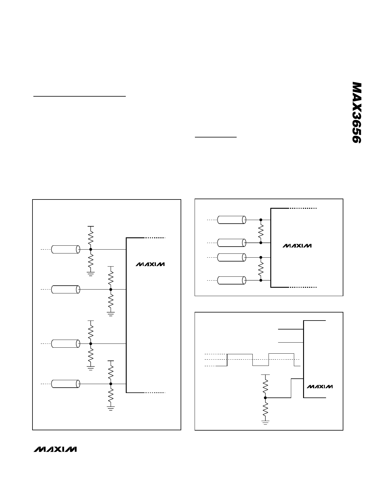
Input Termination Requirements
The MAX3656 data and BEN inputs are internally biased.
Although the inputs are compatible with LVPECL signals,
it is not necessary to drive the MAX3656 with a standard
LVPECL signal. While DC-coupled, the MAX3656 oper-
ates properly as long as the specified common-mode
voltage and differential voltage swings are met.
Because of the on-chip biasing network (Figure 3), the
MAX3656 inputs self-bias to the proper operating point
to accommodate AC-coupling.
See Figures 4 and 5 for connecting to PECL or CML
data outputs.
VCC
VCC
VCC
16kΩ
5kΩ
IN+
VCC
5kΩ
IN-
24kΩ
VCC
BEN+
VCC
16kΩ
5kΩ
MAX3656
VCC
VCC
5kΩ
BEN-
24kΩ
Figure 3. MAX3656 Internal Biasing
______________________________________________________________________________________ 11
Share Link: 