RF3321 Ver la hoja de datos (PDF) - RF Micro Devices
Número de pieza
componentes Descripción
Fabricante
RF3321 Datasheet PDF : 16 Pages
| |||
RF3321
Preliminary
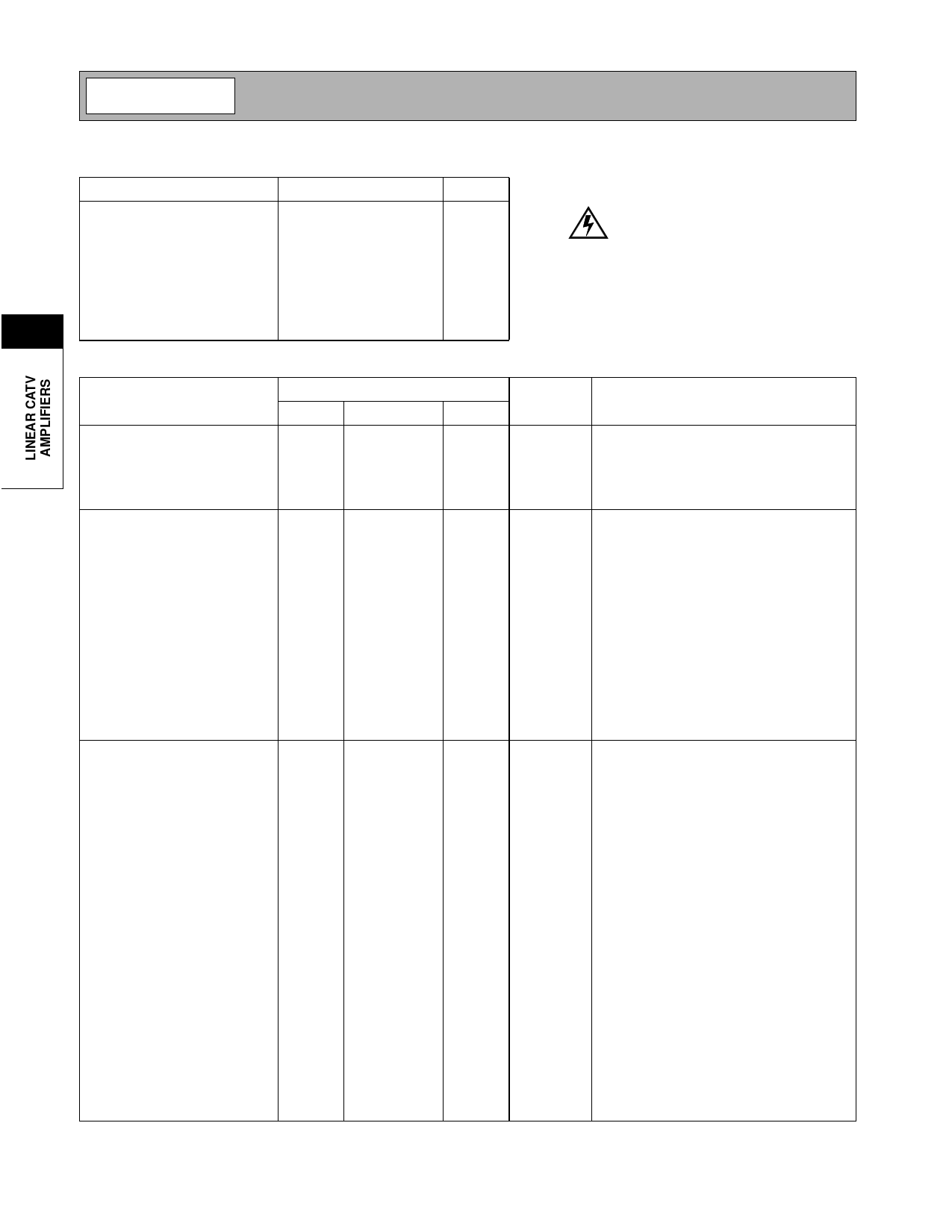
Absolute Maximum Ratings
Parameter
Rating
Supply Voltage (VCC1)
Supply Voltage (VCC2)
Input RF Level
Operating Ambient Temperature
Storage Temperature
Humidity
Maximum Power Dissipation
3
Maximum TJ
-0.5 to +5.5
-0.5 to +7.5
12
-40 to +85
-40 to +150
80
0.5
150
Unit
VDC
VDC
dBm
°C
°C
%
W
°C
Caution! ESD sensitive device.
RF Micro Devices believes the furnished information is correct and accurate
at the time of this printing. However, RF Micro Devices reserves the right to
make changes to its products without notice. RF Micro Devices does not
assume responsibility for the use of the described product(s).
Parameter
Overall
DC Specifications
Supply Voltage 1 (VCC1)
Supply Voltage 2 (VCC2)
Supply Current
Maximum Gain, SV1
Maximum Gain, SV2
Low Gain, SV1
Low Gain, SV2
Transmit Disable
Shut Down
Logic High Voltage
Logic Low Voltage
Logic Leakage Current
AC Specifications
Voltage Gain
Maximum
Minimum
Bandwidth
Maximum Input Level
Maximum Output Level
Output Harmonic Distortion
Output Step Size
Output Noise
Maximum Gain
Minimum Gain
Transmit Disabled
TX EN Enable Time
TX EN Transient Duration
Specification
Min.
Typ.
Max.
4.75
5.0
5.25
6.65
7.0
7.35
85
100
135
150
75
90
55
70
25
35
5
2
0.8
-1
1
Unit
V
V
mA
mA
mA
mA
mA
mA
V
V
µA
Condition
VCC1=5V, VCC2=7V, TXEN=SHDNB=1,
VIN=38dBmV (rms) differential, output
impedance=75Ω through a 2:1 transformer.
Typical performance is at TA=+25°C,
VCC = 5 V.
Main chip supply
Output stage supply
Gain Control Word=56, VCC2=5V or 7V
Gain Control Word=56, VCC2=5V or 7V
Gain Control Word<28, VCC2=5V or 7V
Gain Control Word<28, VCC2=5V or 7V
TXEN=0, VCC2=5V or 7V
SHDNB=0, VCC2=5V or 7V
29
31
dB
Gain Control Word=56, VCC2=5V or 7V
-25
-23
dB
Gain Control Word=0, VCC2=5V or 7V
100
MHz
Intended operating range is 5MHz to
65 MHz.
40
dBmV(rms)
69
dBmV(rms) Into 75Ω load at balun output (CW),
VCC2 = 7 V
65
dBmV VCC2=5V
-56
-50
dBc
Output Level=68dBmV (rms) (CW)
Maximum Gain, VCC2=5V or 7V
0.8
1.0
1.1
dB
-35
-30
dBmV/ VCC2=5V or 7V
160 kHz
-50
-45
dBmV/ VCC2=5V or 7V
160 kHz
-75
-70
dBmV/ TXEN=0, VCC2=5V or 7V
160 kHz
0.5
1.0
µS
Time for gain to reach 99% of final value.
See Note 1.
2.4
3.0
µS
See Note 1.
2-2
Rev A10 010516
Share Link: 