UAA3522 Ver la hoja de datos (PDF) - Philips Electronics
Número de pieza
componentes Descripción
Fabricante
UAA3522 Datasheet PDF : 28 Pages
| |||
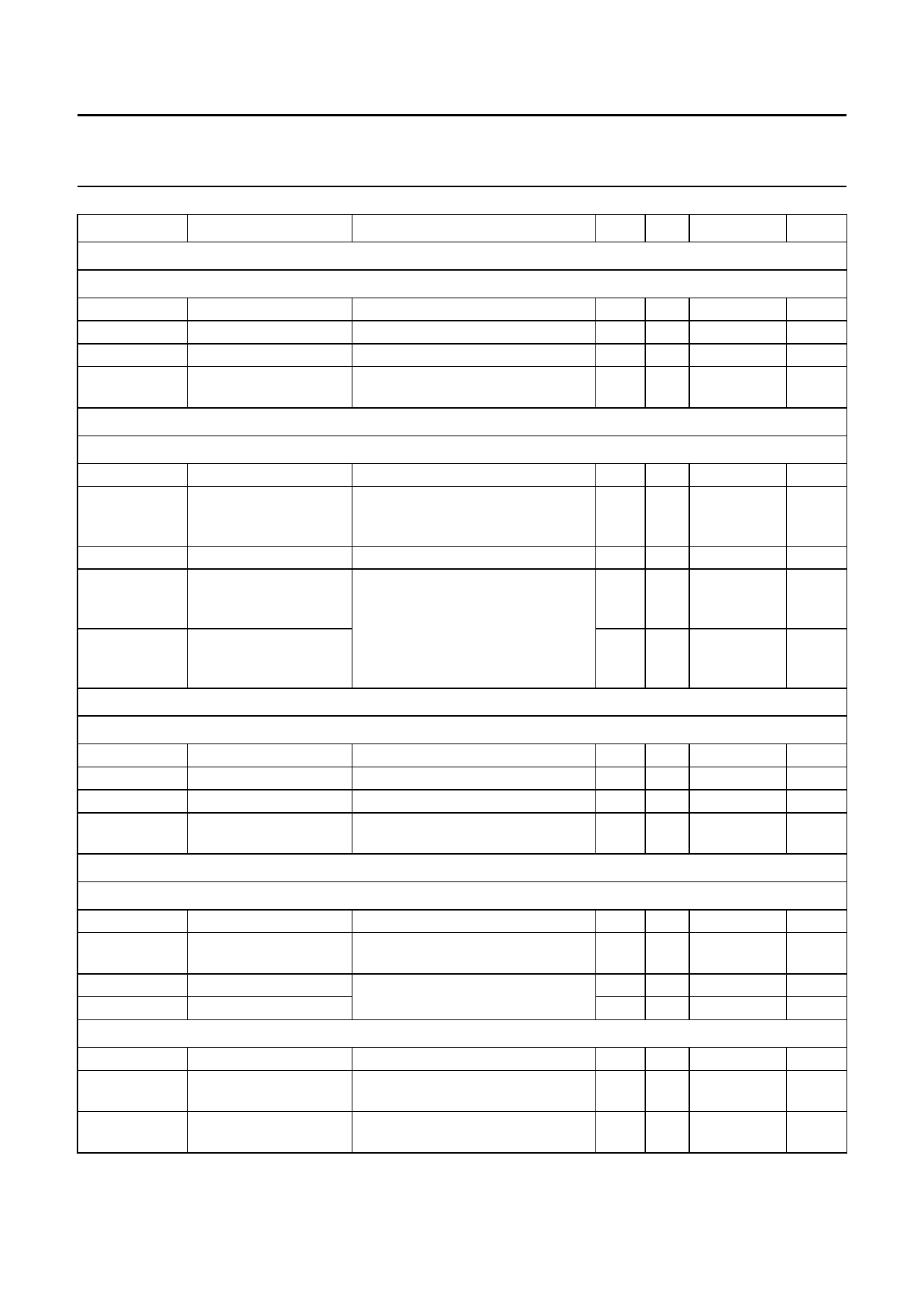
Philips Semiconductors
Low power dual-band GSM transceiver
with an image rejecting front-end
Objective specification
UAA3522HL
SYMBOL
PARAMETER
CONDITIONS
MIN. TYP. MAX.
RF LO buffer; measured and guaranteed on evaluation board
RF LO SOURCE CONNECTED TO PIN RFLOE (see Fig.7)
Ri
Ci
S11
Pi(LO)
input resistance
input capacitance
input power matching
input power acceptable
from the RF LO source
−
50 −
−
1−
−
−15 −10
−7 −3 2
IF LO; measured and guaranteed on evaluation board
EXTERNAL RESONATOR CIRCUIT CONNECTED TO PINS IFLOC AND IFLOE
fosc
oscillation frequency note 1
−
Vosc(peak)
peak voltage excursion VCCIFLO = 2.8 V; see Fig.5
1
limit at IFLOC
(collector)
ϕN
∆fTROFF
phase noise
foffset = 400 kHz; fLO(IF) = 400 MHz −
frequency variation with note 14
−
supply voltage
(pushing)
∆fTRON
frequency variation
−
between RX on and
RX off (pulling)
400 −
− 1.5
− −125
−
1
− 10
IF LO buffer; measured and guaranteed on evaluation board
IF SOURCE CONNECTED TO PIN IFLOE
Ri
Ci
Pi(m)
PIF
input resistance
input capacitance
input power matching
power available from
the IF source
see Fig.5
−
50 −
−
1−
−
−15 −10
−8 −5 −2
RF and IF synthesizer VCOs
REFERENCE FREQUENCY INPUT (PIN REFIN)
fref
Vi(fref)(rms)
reference frequency
input voltage level
(RMS value)
−
13 −
80 − 250
Ri
input resistance
fref = 13 MHz
Ci
input capacitance
−
10 −
−
1−
RF SYNTHESIZER; GSM AND DCS MODES (PINS RXIRFA, RXIRFB AND CPORF)
fLO(RF)
fph(comp)
RF LO frequency
phase comparator
frequency
1040 − 1720
−
200 −
ϕN(GSM)
GSM close-in phase within the closed-loop bandwidth −
noise
Pxtal = 0 dBm; fLO(RF) = 1.1 GHz
−82 −75
UNIT
Ω
pF
dB
dBm
MHz
V
dBc/Hz
MHz/V
kHz
Ω
pF
dB
dBm
MHz
mV
kΩ
pF
MHz
kHz
dBc/Hz
2000 Feb 18
17
Share Link: 