UAA3522 Ver la hoja de datos (PDF) - Philips Electronics
Número de pieza
componentes Descripción
Fabricante
UAA3522 Datasheet PDF : 28 Pages
| |||
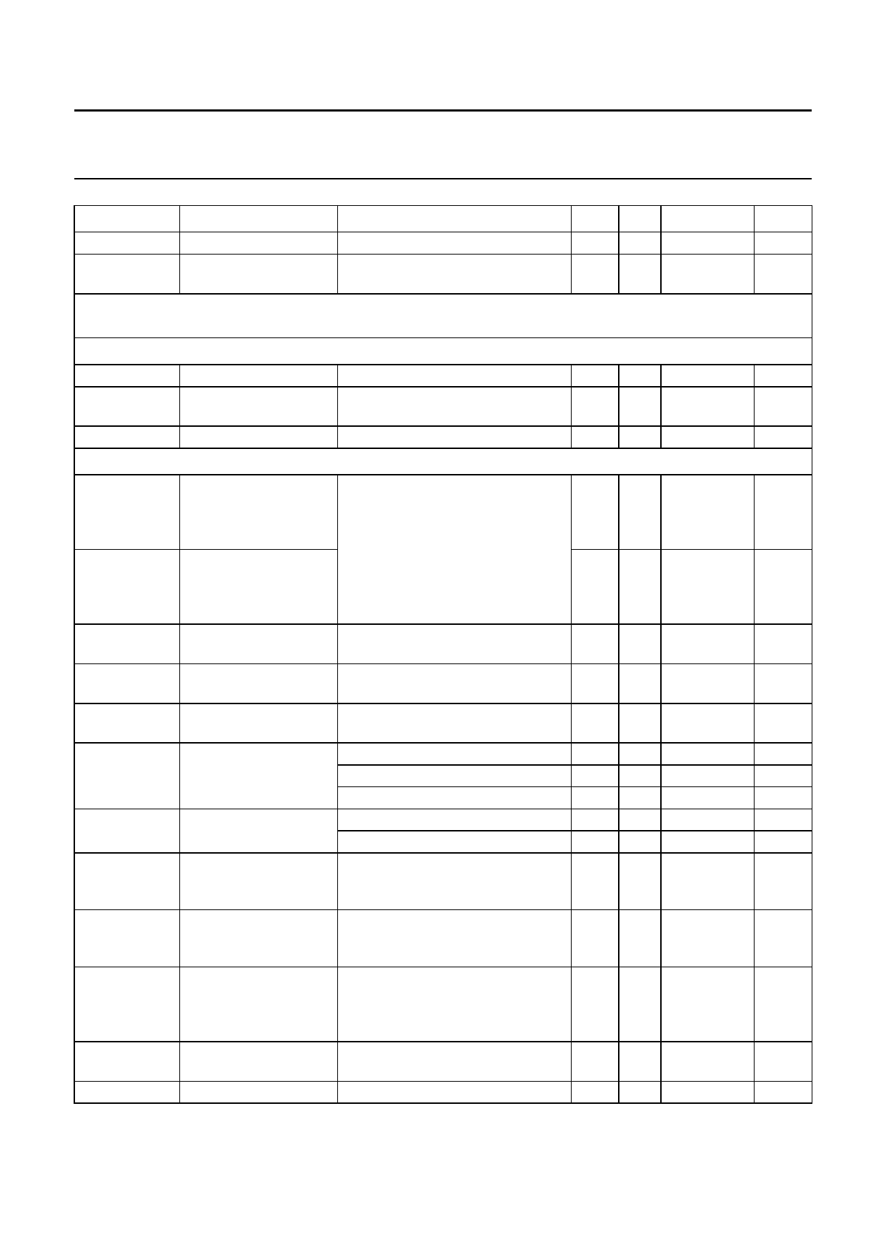
Philips Semiconductors
Low power dual-band GSM transceiver
with an image rejecting front-end
Objective specification
UAA3522HL
SYMBOL
PARAMETER
CONDITIONS
MIN. TYP. MAX.
UNIT
IR
image rejection
fo(IF) = 200 MHz; note 1
30 35 −
dB
Goff
output isolation in
bit LNA = 0; notes 1 and 5
60 70 −
dB
off-state
Receiver IF section (AGC and baseband filter); the impedance of the source, input balun, matching network
and specified input is 50 Ω
IF INPUT TO AGC AMPLIFIER (PINS RXIIFA AND RXIIFB)
fi(IF)
Ri(dif)
IF input frequency
differential input
resistance
Pi(m)
input power matching note 1
BASEBAND INPUT/OUTPUT; RX MODE (PINS IA, IB, QA AND QB)
Gconv(dif)(min)
differential voltage
conversion gain per
channel; gain set to
minimum
notes 1 and 7
Gconv(dif)(max)
differential voltage
conversion gain per
channel; gain set to
maximum
Gconv(step)
voltage conversion step note 1
gain
∆GI-Q
gain difference
note 1
between I and Q paths
∆ϕ
quadrature-phase error
between I and Q paths
GL
gain control linearity note 1
notes 1 and 11
within any 20 dB gain range
F
noise figure
Gconv(dif)(max); notes 1 and 9
Gconv(dif)(min); notes 1 and 9
IP3
third-order intercept
Gconv(dif)(max) = 61 dB; note 8
point referenced to
input
CP1
−1 dB compression
point referenced to
input
Gconv(dif)(min); note 8
CP1adjacent
−1 dB compression
point for adjacent
channels referenced to
input
Gconv = 49 dB; notes 7 and 6
∆fmod = n × 200 kHz; n = 1, 2, 3
Bbf(-1dB)
−1 dB baseband filter note 10
bandwidth
∆td(g)
group delay variation DC < ∆fmod < 67.7 kHz
−
200 −
−
1−
−
−15 −10
−2.5 −0.5 +1.5
59.5 61.5 63.5
−
2−
−
− 0.8
−5 − +5
−2 − +2
−3 − +3
−1 − +1
−
−9
−
− 61
−42 −38 −
−4 0 −
−45 −40 −
67.7 − −
−
1.5 −
MHz
kΩ
dB
dB
dB
dB
dB
deg
dB
dB
dB
dB
dB
dBm
dBm
dBm
kHz
µS
2000 Feb 18
14
Share Link: 