MJL16218 Ver la hoja de datos (PDF) - Motorola => Freescale
Número de pieza
componentes Descripción
Fabricante
MJL16218 Datasheet PDF : 8 Pages
| |||
MOTOROLA
SEMICONDUCTOR TECHNICAL DATA
Order this document
by MJL16218/D
™ Designer's Data Sheet
SCANSWITCH™
NPN Bipolar Power Deflection Transistor
For High and Very High Resolution Monitors
The MJL16218 is a state–of–the–art SWITCHMODE™ bipolar power transistor. It is
specifically designed for use in horizontal deflection circuits for 20 mm diameter neck,
high and very high resolution, full page, monochrome monitors.
• 1500 Volt Collector–Emitter Breakdown Capability
• Typical Dynamic Desaturation Specified (New Turn–Off Characteristic)
• Application Specific State–of–the–Art Die Design
• Fast Switching:
175 ns Inductive Fall Time (Typ)
2000 ns Inductive Storage Time (Typ)
• Low Saturation Voltage:
0.2 Volts at 5.0 Amps Collector Current and 2.0 A Base Drive
• Low Collector–Emitter Leakage Current — 250 µA Max at 1500 Volts — VCES
• High Emitter–Base Breakdown Capability For High Voltage Off Drive Circuits —
8.0 Volts (Min)
MAXIMUM RATINGS
Rating
Collector–Emitter Breakdown Voltage
Collector–Emitter Sustaining Voltage
Emitter–Base Voltage
Collector Current — Continuous
— Pulsed (1)
Base Current — Continuous
— Pulsed (1)
Maximum Repetitive Emitter–Base
Avalanche Energy
Total Power Dissipation @ TC = 25°C
@ TC = 100°C
Derated above TC = 25°C
Operating and Storage Temperature Range
THERMAL CHARACTERISTICS
Characteristic
Thermal Resistance — Junction to Case
Lead Temperature for Soldering Purposes
1/8″ from the case for 5 seconds
(1) Pulse Test: Pulse Width = 5.0 ms, Duty Cycle ≤ 10%.
(2) Proper strike and creepage distance must be provided.
Symbol
VCES
VCEO(sus)
VEBO
IC
ICM
IB
IBM
W (BER)
PD
TJ, Tstg
Symbol
RθJC
TL
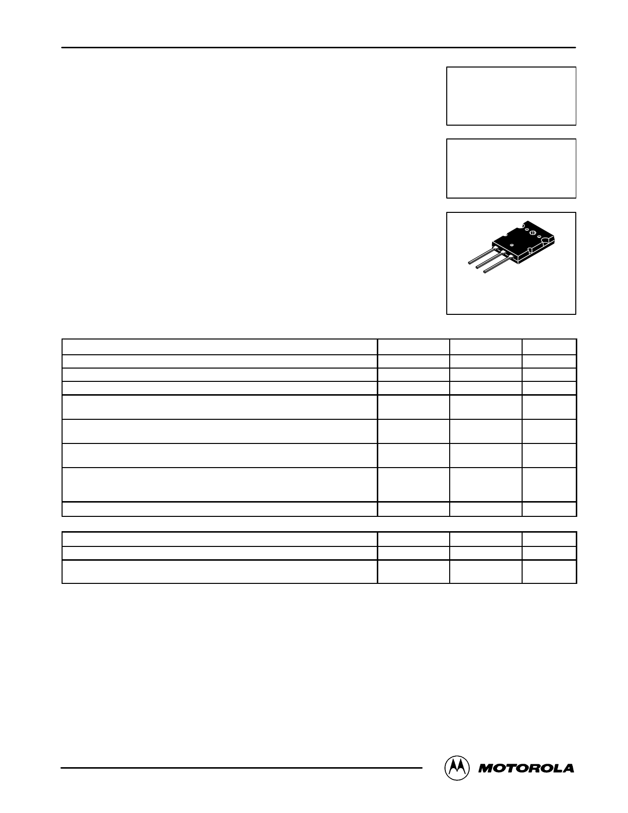
MJL16218*
*Motorola Preferred Device
POWER TRANSISTOR
15 AMPERES
1500 VOLTS — VCES
170 WATTS
CASE 340G–02, STYLE 2
TO–3PBL
Value
1500
650
8.0
15
20
7.0
14
0.2
170
39
1.49
– 55 to 125
Max
0.67
275
Unit
Vdc
Vdc
Vdc
Adc
Adc
mJ
Watts
W/°C
°C
Unit
°C/W
°C
Designer’s and SCANSWITCH are trademarks of Motorola, Inc.
Designer’s Data for “Worst Case” Conditions — The Designer’s Data Sheet permits the design of most circuits entirely from the information presented. SOA Limit
curves — representing boundaries on device characteristics — are given to facilitate “worst case” design.
Preferred devices are Motorola recommended choices for future use and best overall value.
©MMoototorroollaa, IBncip. 1o9la97r Power Transistor Device Data
1
Share Link: 