2N6764 Ver la hoja de datos (PDF) - Omnirel Corp => IRF
Número de pieza
componentes Descripción
Fabricante
2N6764
Omnirel Corp => IRF

2N6764 Datasheet PDF : 5 Pages
| |||
2N6764, JANTX2N6764, JANTXV2N6764
2N6766, JANTX2N6766, JANTXV2N6766
2N6768, JANTX2N6768, JANTXV2N6768
2N6770, JANTX2N6770, JANTXV2N6770
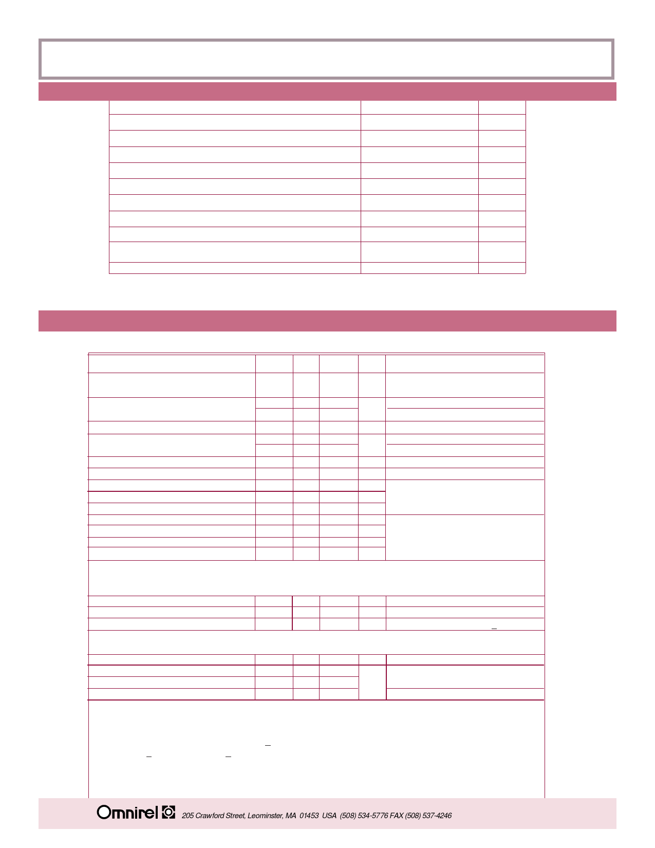
ABSOLUTE MAXIMUM RATINGS (TC = 25°C unless otherwise noted
Parameter
JANTXV, JANTX, 2N6770
Units
ID @ VGS = 10V, TC = 25°C Continuous Drain Current
ID @ VGS = 10V, TC = 100°C Continuous Drain Current
ID M
Pulsed Drain Current1
PD @ TC = 25°C
Maximum Power Dissipation
Linear Derating Factor
12
A
7.75
A
48
A
150
W
1.2
W/°C
VG S
Gate-Source Voltage
± 20
V
EAS
Single Pulse Avalanche Energy 2
8.0 4
mJ
IA R
Avalanche Current1
12 4
A
TJ
Operating Junction
-55 to 150
°C
TS T G
Storage Temperature Range
Lead Temperature
300(.06 from case for 10 sec) °C
ELECTRICAL CHARACTERISTICS @ TJ = 25°C (Unless Otherwise Specified)
Parameter
Min.
BVDSS Drain-Source
500
Breakdown Voltage
RDS(on) Static Drain-to-Source
---
On-State Resistance
---
VGS(th) Gate Threshold Voltage
2.0
IDSS Zero Gate Voltage Drain
---
Current
---
IGSS Gate -to-Source Leakage Forward ---
IGSS Gate -to-Source Leakage Reverse ---
Q G(on) On-state Gate Charge
55
Q G S Gate-to-Source Charge
5.0
Q Gd Gate-to-Drain (“Miller”) Charge
27
tD(on) Turn-On Delay Time
---
tr
Rise Time
---
tD(off) Turn-Off Delay Time
---
tr
Fall Time
---
Typ. Max. Units
V
--- .400
--- .500
---
4.0
V
---
25
µA
--- 250
--- 100 nA
--- -100 nA
--- 120 nC
---
19 nC
---
70 nC
---
35 ns
--- 190 ns
--- 170 ns
--- 130 ns
Test Conditions
VG S =0V,ID =1.0 mA,
VG S = 10 V, ID = 7.75 A 3
VG S = 10 V, ID = 12 A 3
VDS = VG S,ID = 250 µA
VDS = 400 V, VG S = 0V
VDS = 400V, VG S = 0V, TJ = 125°C
VG S = 20 V
VG S = -20 V
VG S = 10 V, ID = 12 A
VDS = 250 V
See note 4
VD D = 250 V, ID = 12 A, RG = 2.35
See note 4
Source-Drain Diode Ratings and Characteristics
Parameter
Min. Typ. Max. Units
VSD Diode Forward Voltage
ttrr
Reverse Recovery Time
---
---
1.7
V
---
--- 1600 ns
Test Conditions
TJ = 25°C, IS = 12A 3,VG S = 0 V
TJ = 25°C, IF= 12A,di/dt<100A/µs 3
Thermal Resistance
Parameter
R thJC
R thCS
R thJA
Junction-to-Case
Case-to-sink
Junction-to-Ambient
Min. Typ. Max. Units
Test Conditions
---
--- 0.83
Mounting surface flat,
--- 0.21 --- °C/W smooth, and greased
---
---
48
Typical socket mount
1. Repetitive Rating: Pulse width limited by maximum junction temperature.
2. @VD D= 50 V, Starting TJ = 25°C, L = 100 µH + 10%, RG = 25 , Peak IL = 12A
3. Pulse width < 300 µs; Duty Cycle < 2 %
4. See MIL-S-19500/543
205 Crawford Street, Leominster, MA 01453 USA (508) 534-5776 FAX (508) 537-4246
Share Link: