FDR6580(1999) Ver la hoja de datos (PDF) - Fairchild Semiconductor
Número de pieza
componentes Descripción
Fabricante
FDR6580 Datasheet PDF : 6 Pages
| |||
Electrical Characteristics TA=25oC unless otherwise noted
Symbol
Parameter
Test Conditions
Min Typ Max Units
OFF CHARACTERISTICS
BVDSS
Drain-Source Breakdown Voltage VGS = 0 V, ID = 250 µA
20
V
IDSS
Zero Gate Voltage Drain Current VDS = 16 V, VGS = 0 V
1
µA
IGSSF
Gate-Body Leakage, Forward
VGS = 8 V, VDS = 0 V
10
µA
IGSSR
Gate-Body Leakage, Reverse
VGS = -8 V, VDS = 0 V
-10
µA
ON CHARACTERISTICS (Note 2)
VGS(TH) Gate Threshold Voltage
VDS = VGS, ID = 250 µA
0.4
1.5
V
RDS(ON)
Static Drain-Source
On-Resistance
VGS = 4.5 V, ID = 11 A
VGS = 2.5 V, ID = 9.3 A
0.009
Ω
0.013
ID(ON)
On-State Drain Current
VGS = 4.5 V, VDS = 5 V
25
A
DRAIN-SOURCE DIODE CHARACTERISTICS AND MAXIMUM RATINGS
IS
Maximum Continuous Drain-Source Diode Forward Current
1.5
A
VSD
Drain-Source Diode Forward
VGS = 0 V, IS = 1.5 A
(Note 2)
Voltage
1.2
V
Notes:
1. RθJA is the sum of the junction-to-case and case-to-ambient resistance where the case thermal reference is defined as the solder mounting surface of
the drain pins. RθJC is guaranteed by design while RθCA is determined by the user's board design.
a) 70° C/W when mounted on a
1.0 in2 pad of 2 oz. copper.
b) 125° C/W when mounted on
a 0.026 in2 pad of 2oz. copper.
c) 135° C/W when mounted
on a minimum pad.
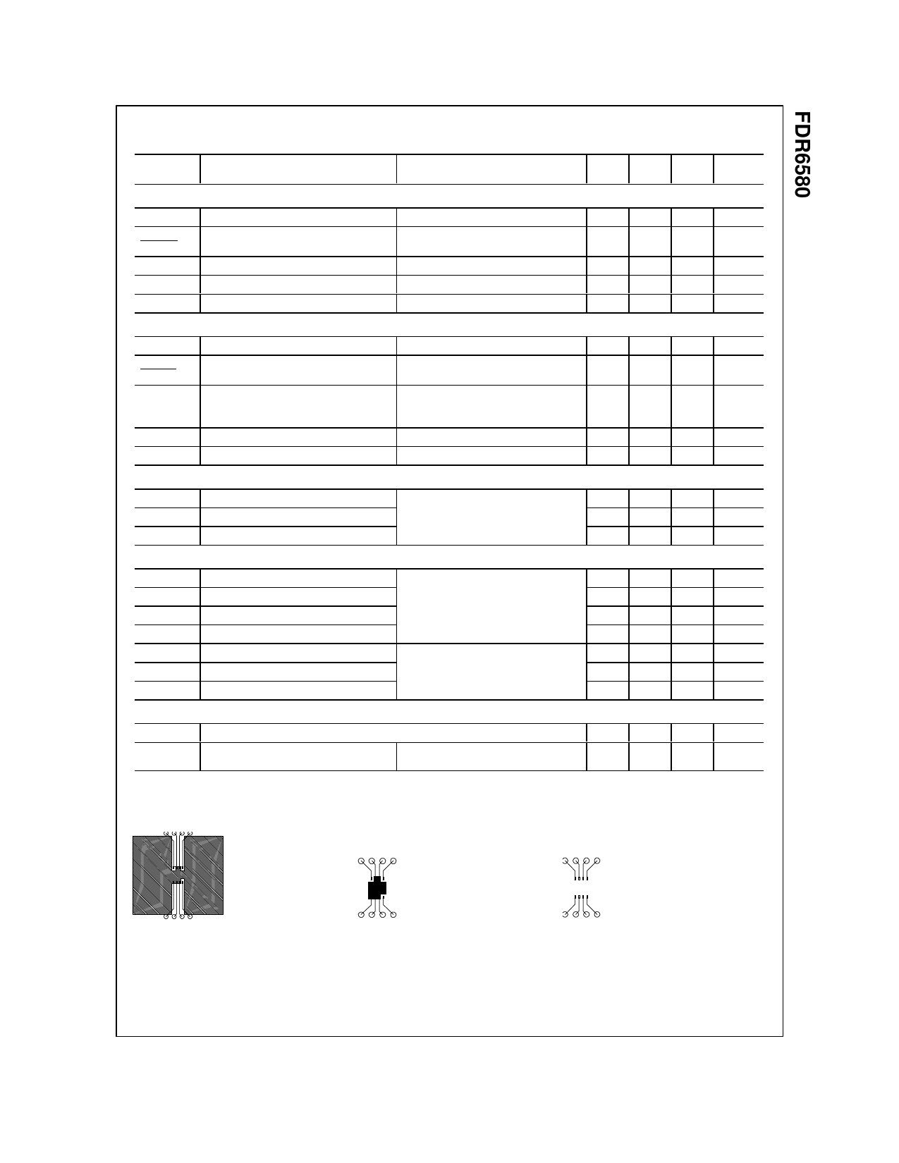
Scale 1 : 1 on letter size paper
2. Pulse Test: Pulse Width ≤ 300 µs, Duty Cycle ≤ 2.0%
FDR6580, Rev. A
Share Link: 