SP8121 Ver la hoja de datos (PDF) - Signal Processing Technologies
Número de pieza
componentes Descripción
Fabricante
SP8121 Datasheet PDF : 13 Pages
| |||
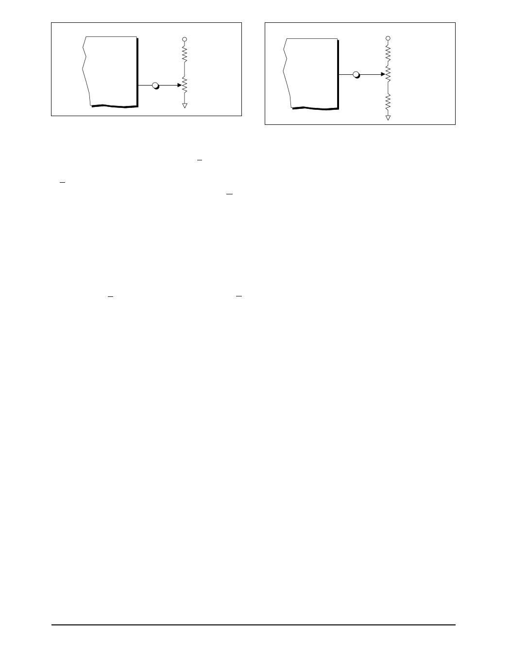
+15V
100K
SP8121
OFFSET ADJUST 6
5K
–1.5mV to +3mV
Figure 1. Offset Adjust
+15V
SP8121
125K
GAIN ADJUST 7
10K
±0.3% Trim Range
Center pot
for zero
correction
19K
Figure 2. Gain Adjust
The conversion cycle is started when R/C is brought
low and must be held low for a minimum of 50ns. The
R/C signal will also put the output latches in a tri-state
mode when low. Approximately 200ns after R/C is
low, STATUS will change from low to high. This
output signal will stay high while the SP8121 is
performing a conversion. Valid data will be latched to
the output bus, through internal control, 500ns prior
to the STATUS line transitioning from a high to low.
READING THE DATA
Please refer to Figure 4. To read data from the
SP8121, the R/C and CE control lines are used. R/C
must be high a minimum of 50ns prior to reading
the data to allow time for the output latches to come
out of the high impedance tri-state mode. CE is used
to access the data. The first 8 MSBs will be on
pins 32 through 25, with pin 32 being the MSB.
The remaining 4 LSBs will be on pins 21 through 24
with pin 21 being the LSB. When CE is switched
from one state to the next, there is a 50ns output
latch propagation delay between the MSBs and LSBs
being present on the output pins.
CALIBRATION
The calibration procedure for the SP8121 consists of
adjusting the most negative input voltage (0V) to the
ideal output code for offset adjustment, and then
adjusting the most positive input voltage (5.0V) to its
ideal output code for gain adjustment.
Offset Adjustment
The offset adjustment must be completed first. Please
refer to Figure 1. Apply an input voltage of 0.5LSB or
610µV to any multiplexer input. Adjust the offset
potentiometer so that the output code fluctuates evenly
between 000…000 and 000…001. It is only
necessary to observe the lower eight LSB’s during this
procedure.
Gain Adjustment
With the offset adjusted, the gain error can now be
trimmed to zero. (Please refer to Figure 2.) The ideal
input voltage corresponding to 1.5 LSB’s below the
nominal full scale input value, or +4.988V, is applied
to any multiplexer input. The gain potentiometer is
adjusted so that the output code alternates evenly
between 111…111 and 111…110. Again, only the
lower eight LSB’s need be observed during this
procedure. With the above adjustment made, the
converter is now calibrated.
SP8121DS/02
SP8121 Monolithic, 12-Bit Data Acquisition System
6
© Copyright 2000 Sipex Corporation
Share Link: 