BGA2031 Ver la hoja de datos (PDF) - Philips Electronics
Número de pieza
componentes Descripción
Fabricante
BGA2031 Datasheet PDF : 12 Pages
| |||
Philips Semiconductors
MMIC variable gain amplifier
Preliminary specification
BGA2031
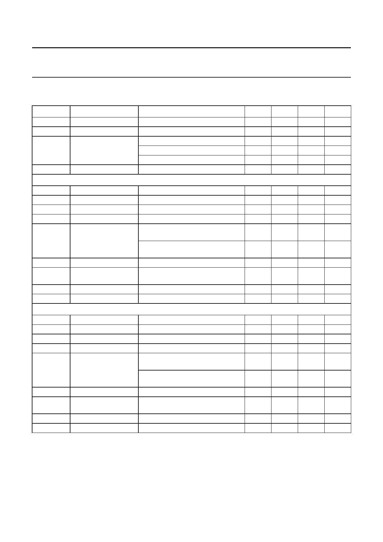
CHARACTERISTICS
Tj = 25 °C; ZS = ZL = 50 Ω; VS = 3.6 V; unless otherwise specified.
SYMBOL
PARAMETER
CONDITIONS
f
VS1, VS2
IS
frequency range
supply voltages
supply current
(in pin 3 + pin 4)
ICTRL
control current
f = 1900 MHz
VCTRL = 0
VCTRL = 2.7 V; VS = 3.6 V
VCTRL = 2.4 V; VS = 3 V
VCTRL = 2.7 V
f
frequency range
GP
power gain
VCTRL = 2.7 V; PL = 12 dBm
∆G
gain control range
0 < VCTRL < 2.7 V
GCS
gain control slope
middle of ∆G
ACPR
adjacent channel power ±1.23 MHz offset; BWACP = 30 kHz;
rejection
BWcarrier = 1.23 MHz; PL = 10 dBm
±1.98 MHz offset; BWACP = 30 kHz;
BWcarrier = 1.23 MHz; PL = 10 dBm
PL
load power
at 1 dB gain compression point
PN
noise power
in CDMA receive band
(1895 − 1955 MHz)
VSWRIN
input VSWR
VCTRL = 2.7 V
VSWROUT output VSWR
VCTRL = 2.7 V
f = 836 MHz
f
GP
∆G
GCS
ACPR
PL
PN
VSWRIN
VSWROUT
frequency range
power gain
gain control range
gain control slope
VCTRL = 2.7 V; PL = 8 dBm
0 < VCTRL < 2.7 V
middle of ∆G
adjacent channel power
rejection
load power
±885 kHz offset; BWACP = 30 kHz;
BWcarrier = 1.23 MHz; PL = 8 dBm
±1.98 MHz offset; BWACP = 30 kHz;
BWcarrier = 1.23 MHz; PL = 8 dBm
at 1 dB gain compression point
noise power
in CDMA receive band
(869 to 894 MHz)
input VSWR
output VSWR
VCTRL = 2.7 V
VCTRL = 2.7 V
MIN.
800
2.7
−
39
23
0.7
TYP.
−
3.6
0
51
30
0.92
MAX.
2 500
4.1
10
63
37
1.1
UNIT
MHz
V
µA
mA
mA
mA
1850 −
−
26
−
61
−
38
−
48
1 950
−
−
−
−
MHz
dB
dB
dB/V
dBc
−
67
−
dBc
−
13.5 −
dBm
−
tbf
−
dBm/Hz
−
1:3.5 −
−
1:1.6 −
824
−
−
27
−
70
−
40
−
55
849
MHz
−
dB
−
dB
−
dB/V
−
dBc
−
69
−
dBc
−
12
−
dBm
−
tbf
−
dBm/Hz
−
1:2
−
−
1:1.7 −
1999 Jul 23
4
Share Link: 