STK672-040 Ver la hoja de datos (PDF) - SANYO -> Panasonic
Número de pieza
componentes Descripción
Fabricante
STK672-040 Datasheet PDF : 11 Pages
| |||
STK672-040
Design material
1. Explanation of input pins
Pin No.
14
15
17
18
9, 10, 11
12, 13
16
8
Name
CLK
CWB
RETURN
ENABLE
M1, M2, M3
M4, M5
RESET
Vref
Function
Phase switching phase
Setting of rotation direction (CW/CCW)
Phase origin forced return
Output cut-off
Setting of exciting mode
Setting of vector locus
System reset
Setting of current value
Pin format
CMOS Schmitt configuration with pull-down resistor
CMOS Schmitt configuration with pull-down resistor
CMOS Schmitt configuration with pull-down resistor
CMOS Schmitt configuration with pull-down resistor
CMOS Schmitt configuration with pull-down resistor
CMOS Schmitt configuration with pull-down resistor
CMOS Schmitt configuration with pull-down resistor
CMOS Schmitt configuration with pull-down resistor
2. Functions and timing of input signals
2-1. CLK (Phase switching clock)
1. Input frequency range sDC to 50 kHz
2. Minimum pulse width s10 µs
3. Duty
s40 to 60%
4. Pin format
sCMOS Schmitt containing pull-up resistor (20 kΩ typical value)
5. Noise eliminating circuit with multiple stages is contained.
6. Functions
a. When the signal M3 is set to 1 or it is opened.
The exciting phase moves at each step at the leading edge of the clock.
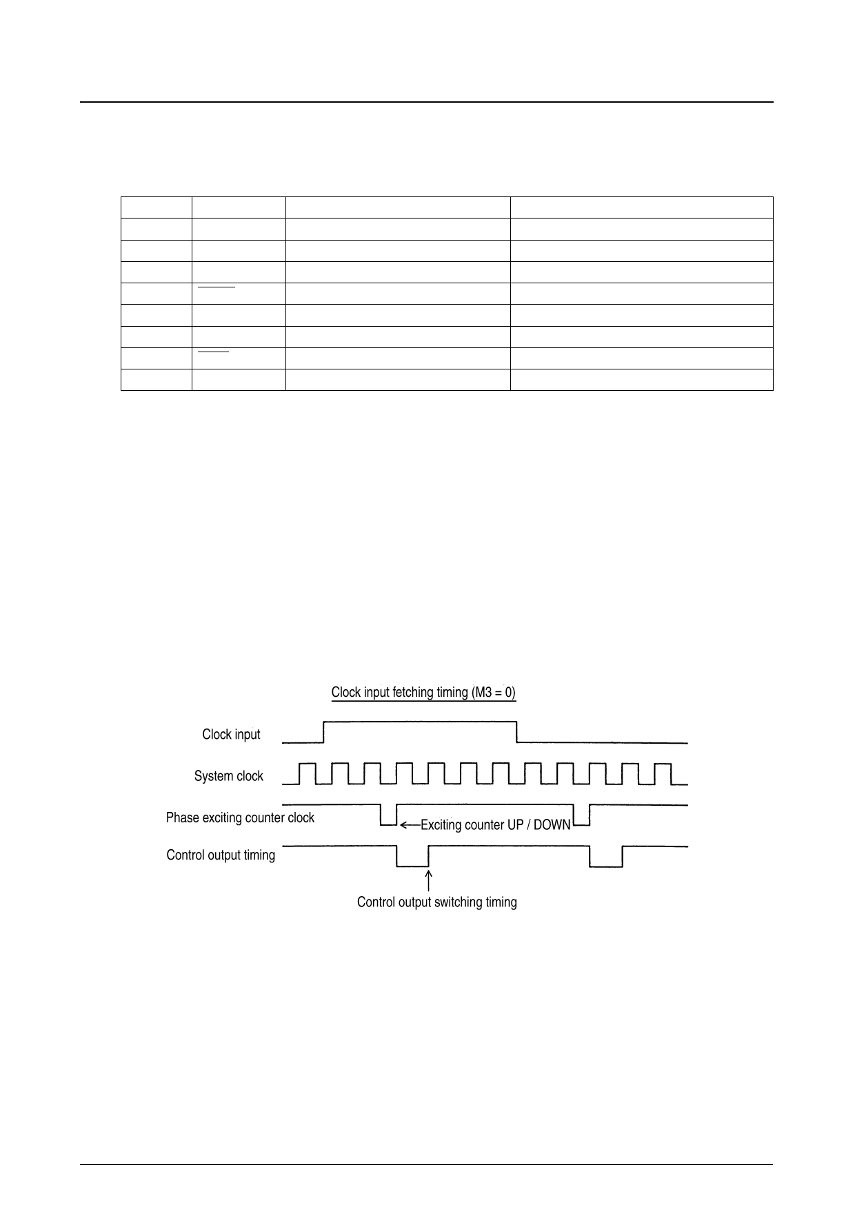
b. When the signal M3 is set to 0
The exciting phase moves at each step at the leading and trailing edges of the clock.
2-2. CWB (Setting of rotation direction)
1. Pin format
sCMOS Schmitt configuration containing pull-up resistor
(20kΩ, typical value)
2. Function
a. When the signal CWB is set to 1
It rotates clockwise.
b. When the signal CWB is set to 0
It rotates counterclockwise.
3. Note
sWhen the signal M3 is set to 0, the CWB input signal must not be changed
at the leading edge and trailing edge of the clock input for the period of 5 µs.
No. 5227—5/11
Share Link: 