MAX697 Ver la hoja de datos (PDF) - Maxim Integrated
Número de pieza
componentes Descripción
Fabricante
MAX697 Datasheet PDF : 16 Pages
| |||
MAX696/MAX697
Microprocessor Supervisory Circuits
Absolute Maximum Ratings
Terminal Voltage (with respect to GND)
VCC.......................................................................-0.3V to +6V
VBATT...................................................................-0.3V to +6V
All Other Inputs (Note 1).....................-0.3V to (VOUT + 0.5V)
Input Current
VCC................................................................................200mA
VBATT..............................................................................50mA
GND.................................................................................20mA
Output Current
VOUT....................................................Short-Circuit Protected
All Other Outputs.............................................................20mA
Rate-of-Rise, VBATT, VCC...............................................100V/μs
Operating Temperature Range
C Suffix................................................................0°C to +70°C
E Suffix.............................................................-40°C to +85°C
M Suffix..........................................................-55°C to +125°C
Power Dissipation (TA = +70°C)
16-Pin PDIP (derated 7mW/°C above +70°C)..............600mW
16-Pin SO (derated 7mW/°C above +70°C).................600mW
16-Pin CERDIP (derated 10mW/°C above +85°C)......600mW
Storage Temperature Range..............................-65°C to +160°C
Lead Temperature (soldering, 10s)..................................+300°C
Note 1: The input voltage limits on PFI and WDI may be exceeded providing the input current is limited to less than 10mA.
Stresses beyond those listed under “Absolute Maximum Ratings” may cause permanent damage to the device. These are stress ratings only, and functional operation of the device at these
or any other conditions beyond those indicated in the operational sections of the specifications is not implied. Exposure to absolute maximum rating conditions for extended periods may affect
device reliability.
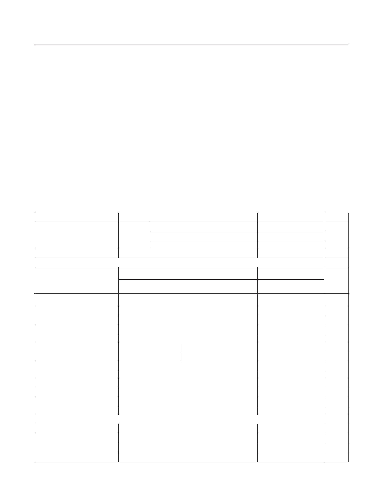
Electrical Characteristics
(VCC = full operating range, VBATT = 2.8V, TA = +25°C, unless otherwise noted.)
PARAMETER
Operating Voltage Range
TA = full
Supply Current (MAX697)
TA = full
BATTERY-BACKUP SWITCHING (MAX696)
CONDITIONS
MAX696 VCC
MAX696 VBATT
MAX697 VCC
VOUT Output Voltage
IOUT = 1mA, TA = full
IOUT = 50mA, TA = full
VOUT in Battery-Backup Mode
IOUT = 250µA, VCC < (VBATT - 0.2V), TA = full
Supply Current (Excludes IOUT)
IOUT = 1mA
IOUT = 50mA
Supply Current in Battery-Backup VCC = 0V, VBATT = 2.8V, TA = +25°C
Mode
VCC = 0V, VBATT = 2.8V, TA = full
Battery Standby Leakage Current
5.5V > VCC > (VBATT +
0.3V)
TA = +25°C
TA = full
Battery Switchover Threshold VCC Power-up
- VBATT
Power-down
Battery Switchover Hysteresis
BATT ON Output Voltage
ISINK - 1.6mA
BATT ON Output Short-Circuit
Current
BATT ON = VOUT = 2.4V sink current
BATT ON = VOUT, VCC = 0V
RESET AND WATCHDOG TIMER
Low-Line Voltage Threshold (LLIN) VCC = +5V, +3V; TA = full
Reset Timeout Delay
Figure 6, OSC SEL HIGH, VCC = 5V
Watchdog Timeout Period,
Internal Oscillator
Long period, VCC = 5V
Short period, VCC = 5V
MIN TYP MAX UNITS
3.0
5.5
2.0
VCC - 0.3V V
3.0
5.5
160 300
µA
VCC - VCC -
0.3
0.1
VCC - VCC -
V
0.5
0.25
VBATT - VBATT
0.1 - 0.02
V
1.5
4
mA
2.5
7
0.6
1
µA
10
-100
+20
nA
-1.00
+0.02 µA
70
mV
50
20
mV
0.4
V
7
mA
0.5
2.5 25.0
µA
1.25 1.30 1.35
V
35
50
70
ms
1.00
1.6
2.25
s
70
100 140
ms
www.maximintegrated.com
Maxim Integrated │ 2
Share Link: 