HT815D0 Ver la hoja de datos (PDF) - Holtek Semiconductor
Número de pieza
componentes Descripción
Fabricante
HT815D0 Datasheet PDF : 15 Pages
| |||
HT815D0
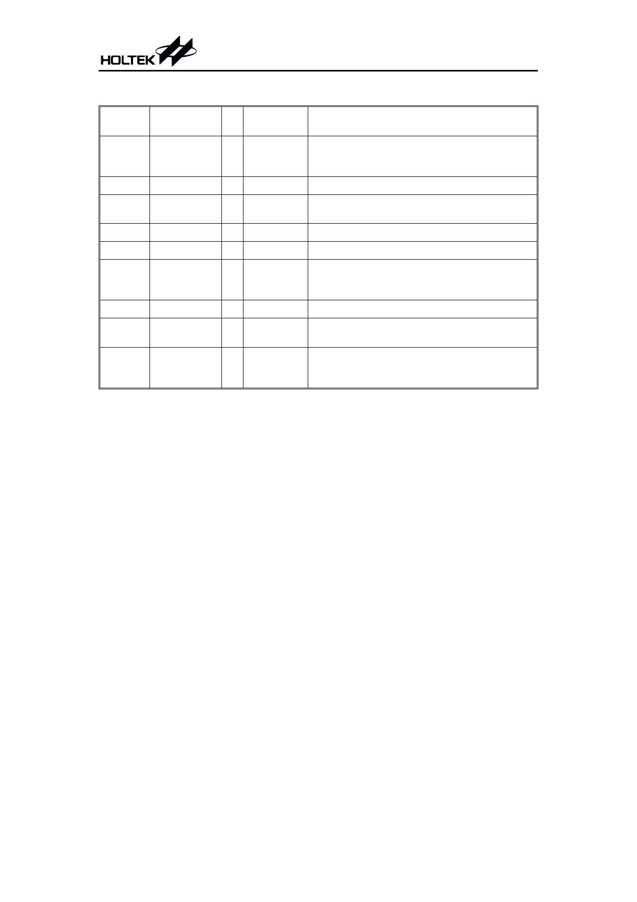
Pad Description
Pad No.
Pad Name
I/O
Internal
Connection
Description
Trigger key, active low. Key features such as
1~3
KEY10~KEY12 I Pull-high debounce time, pull-high resistance and repeat are
all by mask option.
4
VDD
¾
¾
Positive power supply
5
AUD
O
PMOS
Open Drain
Voice output for driving an external transistor
6
OSC2
O
¾
Oscillator output pin
7
OSC1
I
¾
Oscillator input pin
8
FLAG1
O
NMOS
Open Drain
3HzB/6HzB flash output, busy output, end-pulse
or voice output indication (by mask option). Open
drain, active low output
9
VSS
¾
¾
Negative power supply, ground
10
FLAG2
O
NMOS 3Hz/6Hz flash output or busy output (by mask op-
Open Drain tion). Open drain, active low output
Trigger key, active low. Key features such as
11~19 KEY1~KEY9 I Pull-high debounce time, pull-high resistance and repeat are
all by mask option.
Absolute Maximum Ratings
Supply Voltage ............................... -0.3V to 6V
Input Voltage ............... VSS-0.3V to VDD+0.3V
Storage Temperature ............... -50°C to 125°C
Operating Temperature ............ -20°C to 70°C
Note: These are stress ratings only. Stresses exceeding the range specified under ²Absolute Maxi-
mum Ratings² may cause substantial damage to the device. Functional operation of this device
at other conditions beyond those listed in the specification is not implied and prolonged expo-
sure to extreme conditions may affect device reliability.
4
March 15, 2000
Share Link: 