MUR3060CTRF Ver la hoja de datos (PDF) - Thinki Semiconductor Co., Ltd.
Número de pieza
componentes Descripción
Fabricante
MUR3060CTRF
Thinki Semiconductor Co., Ltd.

MUR3060CTRF Datasheet PDF : 2 Pages
| |||
MUR3020CTRF thru MUR3060CTRF
Pb Free Plating Product
MUR3020CTRF/MUR3040CTRF/MUR3060CTRF
Pb
30.0 Ampere Insulated Dual Common Anode Ultra Fast Recovery Rectifiers
Features
Fast switching for high efficiency
Low forward voltage drop
High current capability
Low reverse leakage current
High surge current capability
Application
Automotive Inverters and Solar Inverters
Plating Power Supply,SMPS and UPS
Car Audio Amplifiers and Sound Device Systems
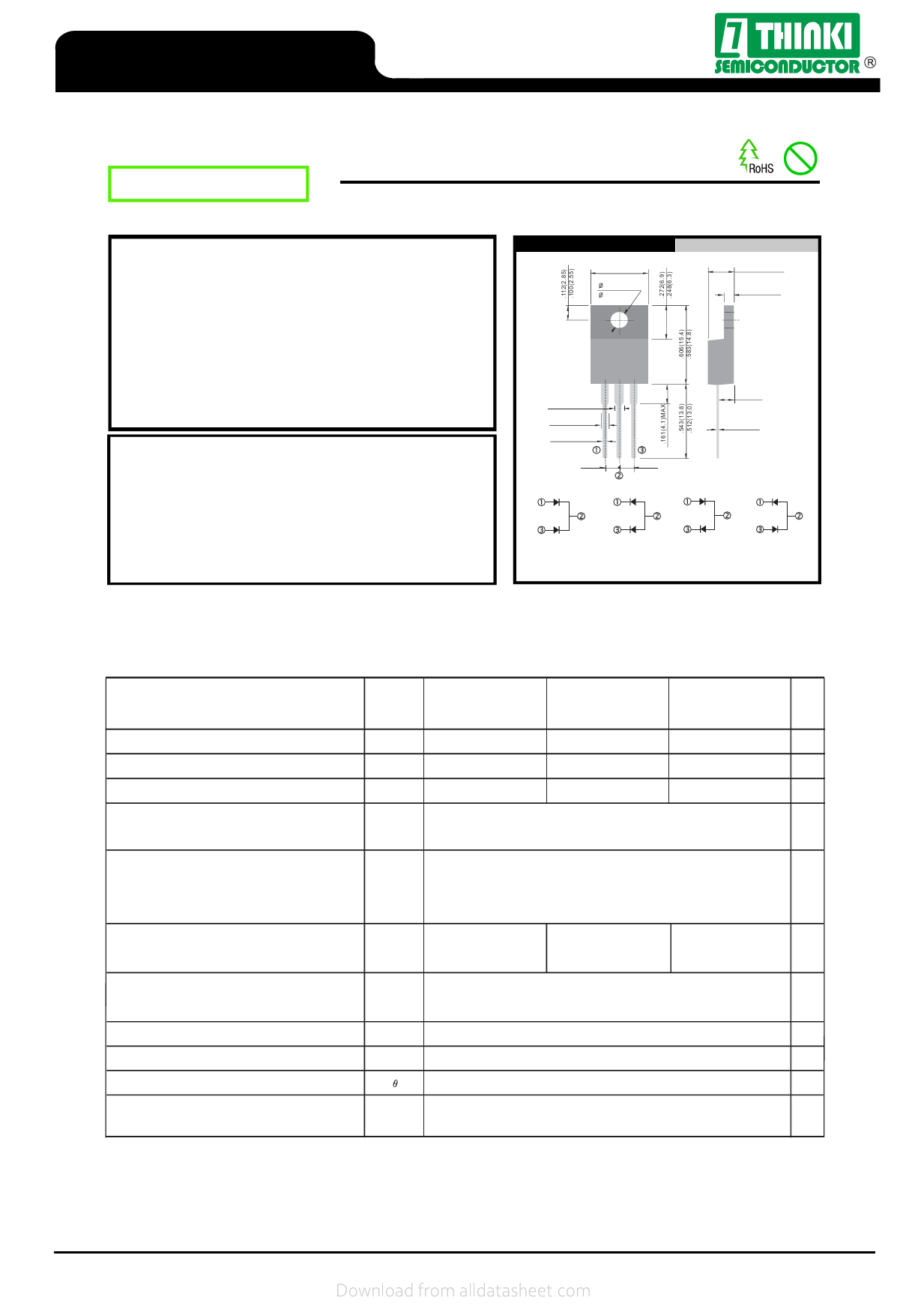
Mechanical Data
Case: ITO-220AB full plastic isolated package
Epoxy: UL 94V-0 rate flame retardant
Terminals: Solderable per MIL-STD-202
method 208
Polarity: As marked on diode body
Mounting position: Any
Weight: 2.1 gram approximately
ITO-220AB/TO-220F-3L
.406(10.3)
.381(9.7)
.134(3.4)
.118(3.0)
Unit : inch (mm)
.189(4.8)
.165(4.2)
.130(3.3)
.114(2.9)
.071(1.8)
.055(1.4)
.055(1.4)
.039(1.0)
.035(0.9)
.011(0.3)
.1
(2.55)
.1
(2.55)
.114(2.9)
.098(2.5)
.032(.8)
MAX
Case
Case
Case
Case
Positive
Negative
Doubler
Series
Common Cathode Common Anode Tandem Polarity Tandem Polarity
Suffix "CTF" Suffix "CTRF" Suffix "CTDF" Suffix "CTSF"
MAXIMUM RATINGS AND ELECTRICAL CHARACTERISTICS
Rating at 25℃ ambient temperature unless otherwise specified.
Single phase, half wave, 60Hz, resistive or inductive load.
For capacitive load, derate current by 20%.
SYMBOL MUR3020CTRF MUR3040CTRF MUR3060CTRF UNIT
Maximum Recurrent Peak Reverse Voltage VRRM
200
Maximum RMS Voltage
VRMS
140
Maximum DC Blocking Voltage
VDC
200
Maximum Average Forward Rectified
Current TC=125 ℃(Total Device 2x15A=30A) IF(AV)
400
600
V
280
420
V
400
600
V
30.0
A
Peak Forward Surge Current, 8.3ms single
Half sine-wave superimposed on rated load IFSM
(JEDEC method)
300
A
Maximum Instantaneous Forward Voltage
VF
0.98
1.3
@ 15A (Per Diode/Per Leg)
1.7
V
Maximum DC Reverse Current @TJ=25℃
IR
5.0
At Rated DC Blocking Voltage @TJ=125℃
100
Maximum Reverse Recovery Time (Note 1) Trr
Typical junction Capacitance (Note 2)
CJ
35-50
150
Typical Thermal Resistance (Note 3)
Operating Junction and Storage
Temperature Range
R JC
TJ, TSTG
3.0
-55 to + 150
NOTES : (1) Reverse recovery test conditions IF= 0.5A, IR = 1.0A, Irr = 0.25A.
(2) Measured at 1.0 MHz and applied reverse voltage of 4.0 Volts DC.
(3) Thermal Resistance junction to case.
μA
μA
nS
pF
℃/W
℃
Rev.09T
© 1995 Thinki Semiconductor Co., Ltd.
Page 1/2
http://www.thinkisemi.com.tw/
Share Link: