HM100N02K Ver la hoja de datos (PDF) - Unspecified
Número de pieza
componentes Descripción
Fabricante
HM100N02K Datasheet PDF : 6 Pages
| |||
.341
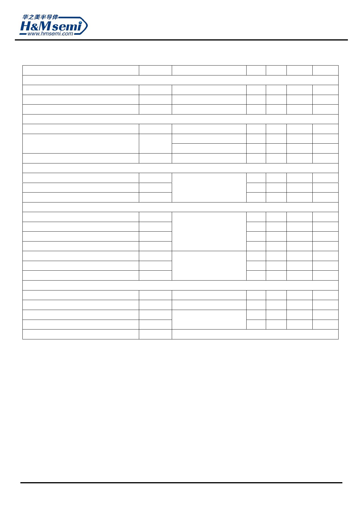
Electrical Characteristics (TC=25℃unless otherwise noted)
Parameter
Symbol
Condition
Min Typ Max Unit
Off Characteristics
Drain-Source Breakdown Voltage
BVDSS
VGS=0V ID=250μA
20
-
-
V
Zero Gate Voltage Drain Current
IDSS
VDS=20V,VGS=0V
-
-
1
μA
Gate-Body Leakage Current
On Characteristics (Note 3)
IGSS
VGS=±12V,VDS=0V
-
-
±100
nA
Gate Threshold Voltage
VGS(th)
VDS=VGS,ID=250μA
0.45 0.65
1.5
V
Drain-Source On-State Resistance
RDS(ON)
VGS=10V, ID=40 A
VGS=4.5V, ID=30A
-
4.5
5.5
mΩ
6.5
7.5
mΩ
Forward Transconductance
Dynamic Characteristics (Note4)
gFS
VDS=10V,ID=40A
15
-
-
S
Input Capacitance
Output Capacitance
Reverse Transfer Capacitance
Switching Characteristics (Note 4)
Clss
- 2000
-
PF
VDS=10V,VGS=0V,
Coss
-
500
-
PF
F=1.0MHz
Crss
-
200
-
PF
Turn-on Delay Time
td(on)
-
6.4
-
nS
Turn-on Rise Time
Turn-Off Delay Time
tr
VDD=10V,ID=2A,RL=1Ω
- 17.2
-
nS
td(off)
VGS=4.5V,RG=3Ω
- 29.6
-
nS
Turn-Off Fall Time
tf
- 16.8
-
nS
Total Gate Charge
Gate-Source Charge
Gate-Drain Charge
Qg
-
27
nC
VDS=10V,ID=40A,
Qgs
-
6.5
nC
VGS=10V
Qgd
-
6.4
nC
Drain-Source Diode Characteristics
Diode Forward Voltage (Note 3)
Diode Forward Current (Note 2)
VSD
VGS=0V,IS=20A
-
1.2
V
IS
-
-
100
A
Reverse Recovery Time
Reverse Recovery Charge
trr
TJ = 25°C, IF = 40A
-
25
-
nS
Qrr
di/dt = 100A/μs(Note3)
-
24
-
nC
Forward Turn-On Time
ton
Intrinsic turn-on time is negligible (turn-on is dominated by LS+LD)
Notes:
1. Repetitive Rating: Pulse width limited by maximum junction temperature.
2. Surface Mounted on FR4 Board, t ≤ 10 sec.
3. Pulse Test: Pulse Width ≤ 300μs, Duty Cycle ≤ 2%.
4. Guaranteed by design, not subject to production
5. EAS condition : Tj=25℃,VDD=10V,VG=10V,L=0.5mH,Rg=25Ω,
Share Link: 