M5M51016RT-10VL-I Ver la hoja de datos (PDF) - MITSUBISHI ELECTRIC
Número de pieza
componentes Descripción
Fabricante
M5M51016RT-10VL-I Datasheet PDF : 7 Pages
| |||
9 Jul ,1997
MITSUBISHI LSIs
M5M51016BTP,RT-10VL-I,
-10VLL-I
1048576-BIT(65536-WORD BY 16-BIT)CMOS STATIC RAM
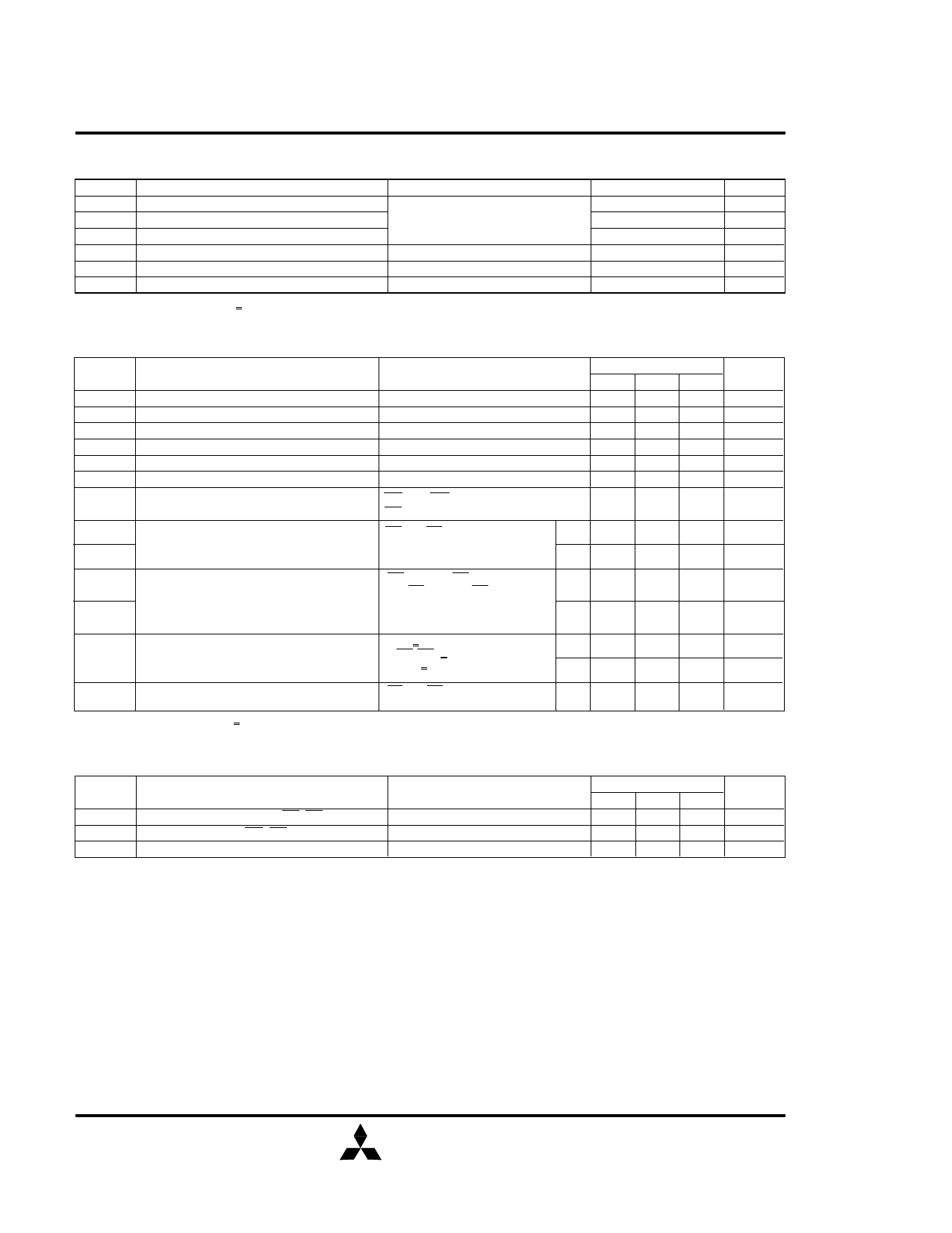
ABSOLUTE MAXIMUM RATINGS
Symbol
Parameter
Vcc
Supply voltage
VI
Input voltage
VO
Output voltage
Pd
Power dissipation
Topr
Operating temperature
Tstg
Storage temperature
* –3.0V in case of AC ( Pulse width < 50ns )
Conditions
With respect to GND
Ta=25 oC
Ratings
Unit
– 0.3 ~ 4.6
V
– 0.3* ~ Vcc + 0.3
V
0 ~ Vcc
V
1
W
– 40 ~ 85
oC
– 65 ~ 150
oC
DC ELECTRICAL CHARACTERISTICS (Ta= -40 ~85 oC, Vcc=3.3V _+ 0.3V, unless otherwise noted)
Symbol
Parameter
VIH
VIL
VOH1
VOH2
VOL
II
IO
High-level input voltage
Low-level input voltage
High-level output voltage 1
High-level output voltage 2
Low-level output voltage
Input current
Output current in off-state
ICC1W
ICC2W
Word operation (16bit)
Active supply current
(AC,TTL level)
Test conditions
Limits
Min Typ Max
Unit
IOH = – 1mA
IOH = – 0.1mA
IOL = 2mA
VI =0 ~ Vcc
2.0
– 0.3*
2.4
Vcc–0.5V
Vcc+0.3V
V
0.6
V
V
V
0.4
V
_+1
µA
BC1 and BC2 = VIH or CS = VIL or
OE = VIH, VI/O = 0 ~ Vcc
BC1 and BC2 = VIL, CS = VIH
other inputs = VIH or VIL
Output-open(duty 100%)
Min
cycle
1MHz
_+1
µA
50
mA
12
mA
ICC1B
ICC2B
Byte operation (8bit)
Active supply current
(AC,TTL level)
ICC3
Stand-by current
ICC4
Stand-by current
* –3.0V in case of AC ( Pulse width < 30ns )
(BC1 = VIH and BC2 = VIL)
or (BC1 = VIL and BC2 = VIH),
CS = VIH
other inputs = VIH or VIL
Output-open(duty 100%)
1) CS < 0.2V, other inputs = 0~Vcc
2) BC1,BC2 > Vcc - 0.2V,
CS > Vcc - 0.2V
other inputs = 0~Vcc
BC1 and BC2 = VIH or CS = VIL,
other inputs = 0~Vcc
Min
cycle
1MHz
-VL
-VLL
30
mA
10
mA
120
µA
24
µA
1
mA
CAPACITANCE (Ta= -40 ~ 85oC , Vcc=3.3V _+ 0.3V, unless otherwise noted)
Symbol
Parameter
CI
Input capacitance ( except BC1,BC2)
CIBC
Input capacitance ( BC1,BC2 )
CO
Output capacitance
Note 1: Direction for current flowing into an IC is positive (no mark).
2: Typical value is Vcc = 3.3V, Ta = 25oC
Test conditions
VI=GND, VI=25mVrms, f=1MHz
VI=GND, VI=25mVrms, f=1MHz
VO=GND,VO=25mVrms, f=1MHz
Limits
Min Typ Max
Unit
6
pF
9
pF
8
pF
MITSUBISHI
ELECTRIC
3
Share Link: 