L9348 Ver la hoja de datos (PDF) - STMicroelectronics
Número de pieza
componentes Descripción
Fabricante
L9348 Datasheet PDF : 13 Pages
| |||
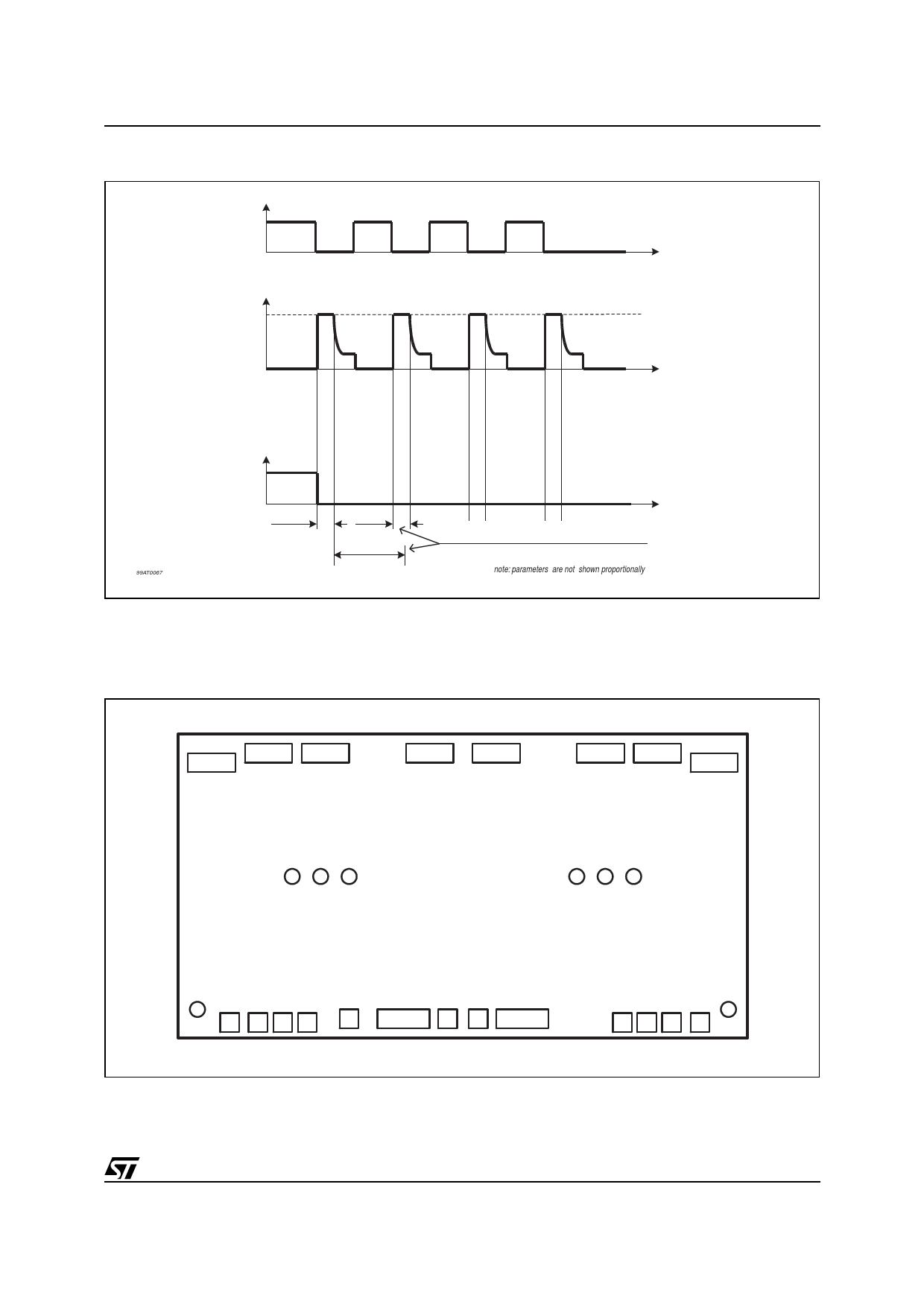
Figure 9. Output Voltage Clamp Detection
VIN3/4
VQ3/4
VZ
L9348
t
t
99AT0067
VST3/4
tclamp
tclamp
tD
3.0 PAD POSITIONS
Chip Size: 5.17 x 2.76 mm2
Figure 10.
PGND4
Q4
D4
Q2
t
note: parameters are not shown proportionally
time between two clamping periods is
shorter than internal delay time
-> status signal remains low
Q1
D3
Q3
PGND3
ST4 IN2 IN4 ST2
ENA
PGND2 GND VS PGND1
ST1 IN3 IN1 ST3
11/13
Share Link: 