MAX44260(2011) Ver la hoja de datos (PDF) - Maxim Integrated
Número de pieza
componentes Descripción
Fabricante
MAX44260 Datasheet PDF : 14 Pages
| |||
MAX44260/MAX44261
1.8V 15MHz Low-Offset,
Low-Power, Rail-to-Rail I/O Op Amps
Applications Information
Power-Up Autotrim
The ICs feature an automatic trim that self-calibrates the
VOS of these devices to less than 100FV of input offset
voltage on power-up. This self-calibration feature allows
the device to eliminate input offset voltage effects due
to power supply and operating temperature variation
simply by cycling its power. The autotrim sequence takes
approximately 10ms to complete and is triggered by an
internal power-on-reset (POR) circuitry. During this time,
the inputs and outputs are put into high impedance and
left unconnected. The MAX44261 can also be forced into
a self-calibration cycle by pulling the CAL input low for
1ms. This input also puts the part into shutdown mode.
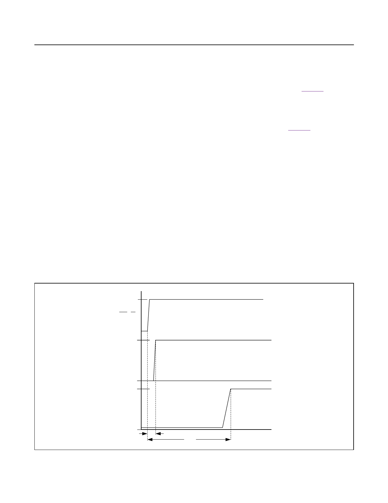
Shutdown Operation
The MAX44260 features an active-low shutdown mode
that puts both inputs and outputs into high impedance
and substantially lowers the quiescent current to less
than 1FA. Putting the output into high impedance allows
multiple outputs to be multiplexed onto a single output
line without the additional external buffers. The device
does not self-calibrate when exiting shutdown mode
and retains its power-up trim settings. Figure 3 shows
that the device also recovers from shutdown in under
30Fs.
The MAX44261 features a recalibrate input that acts the
same as the shutdown mode of the MAX44260. However,
when the input is pulled low, the device goes through a
self-calibration sequence again (Figure 3).
The shutdown logic levels of the devices are indepen-
dent of supply, allowing the shutdown feature of the
device to operate off of a 1.8V or 3.3V microcontroller,
regardless of supply voltage.
Rail-to-Rail Input/Output
The input voltage range of the ICs extends 100mV
above VDD and below VSS. The wide input common-
mode voltage range allows the op amp to be used as
a buffer and as a differential amplifier in a wide-variety
of signal processing applications. Output voltage high/
low is designed to be only 50mV above VSS and below
VDD allowing maximum dynamic range in single-supply
applications. The high output current and capacitance
drive capability of the devices make them ideal as an
ADC driver and a line driver.
VDD
VSHDN/VCAL
0V
VDD/2
MAX44260
OUTPUT
0V
VDD/2
MAX44261
OUTPUT
FAST RECOVERY
AMPLIFIER
ACTIVE
AUTOTRIM
SEQUENCE
RECALIBRATED
AMPLIFIER
ACTIVE
0V
30µs
10ms
Figure 3. CAL vs. SHDN Input Operation
���������������������������������������������������������������� Maxim Integrated Products 11
Share Link: 