PS22053 Ver la hoja de datos (PDF) - MITSUBISHI ELECTRIC
Número de pieza
componentes Descripción
Fabricante
PS22053 Datasheet PDF : 9 Pages
| |||
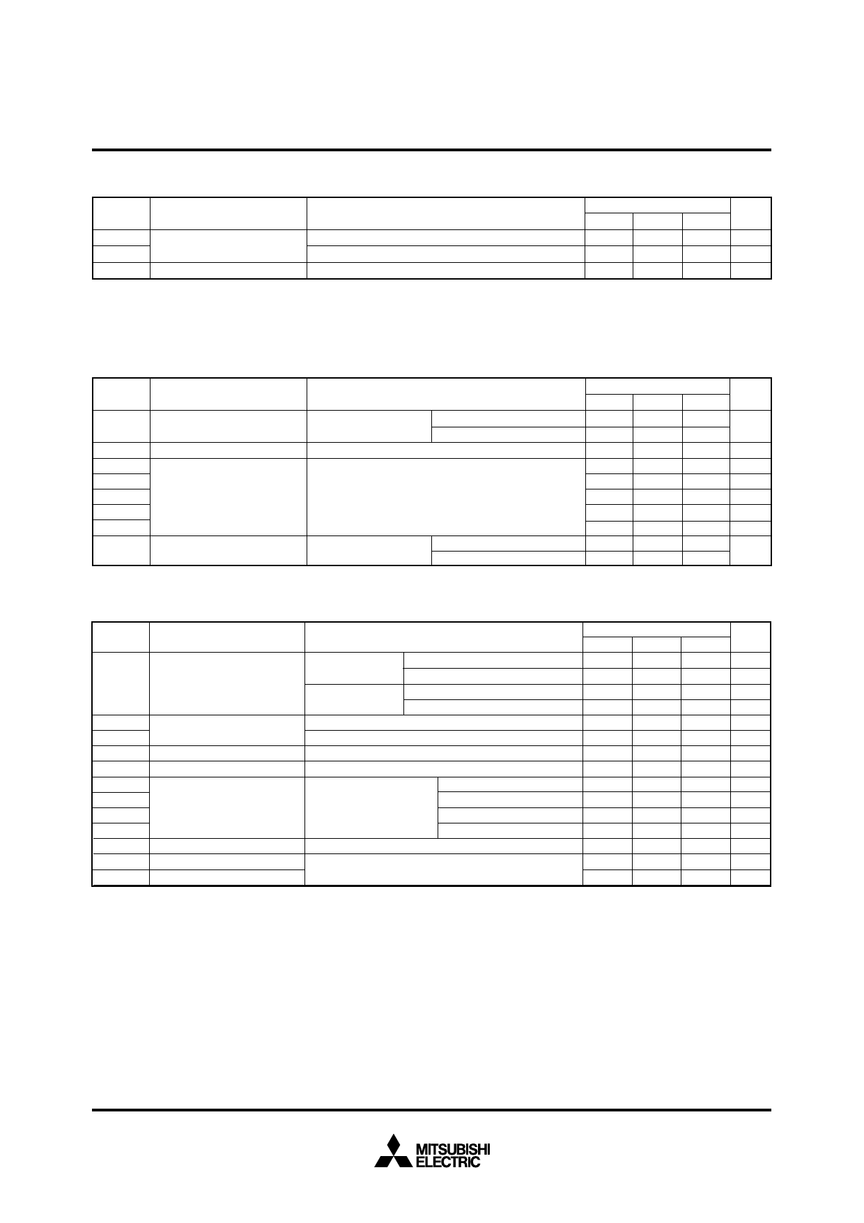
MITSUBISHI SEMICONDUCTOR <Dual-In-Line Package Intelligent Power Module>
PS22053
TRANSFER-MOLD TYPE
INSULATED TYPE
THERMAL RESISTANCE
Symbol
Parameter
Condition
Limits
Min.
Typ.
Max. Unit
Rth(j-c)Q
Rth(j-c)F
Junction to case thermal
resistance
Inverter IGBT part (per 1/6 module)
Inverter FWDi part (per 1/6 module)
—
—
2.00 °C/W
—
—
2.67 °C/W
Rth(c-f) Contact thermal resistance (Note 3) Case to fin, (per 1 module) thermal grease applied
—
—
0.047 °C/W
Note 3: Grease with good thermal conductivity and long-term endurance should be applied evenly with about +100µm~+200µm on the con-
tacting surface of DIP-IPM and heat-sink.
ELECTRICAL CHARACTERISTICS (Tj = 25°C, unless otherwise noted)
INVERTER PART
Symbol
Parameter
VCE(sat)
VEC
ton
trr
tc(on)
toff
tc(off)
ICES
Collector-emitter saturation
voltage
FWDi forward voltage
Switching times
Collector-emitter cut-off
current
Condition
VD = VDB = 15V
VIN = 5V, IC = 10A
–IC = 10A, VIN = 0V
Tj = 25°C
Tj = 125°C
VCC = 600V, VD = VDB = 15V
IC = 10A, Tj = 125°C, VIN = 0 ↔ 5V
Inductive load (upper-lower arm)
VCE = VCES
Tj = 25°C
Tj = 125°C
Limits
Unit
Min.
Typ.
Max.
—
2.7
3.4
—
2.5
3.2
V
—
2.5
3.0
V
0.8
1.5
2.2
µs
—
0.2
—
µs
—
0.4
0.7
µs
—
2.8
3.8
µs
—
0.4
0.7
µs
—
—
1
mA
—
—
10
CONTROL (PROTECTION) PART
Symbol
Parameter
Condition
Limits
Unit
Min.
Typ.
Max.
ID
Circuit current
VD = VDB = 15V Total of VP1-VPC, VN1-VNC
—
VIN = 5V
VUFB-VUFS, VVFB-VVFS, VWFB-VWFS —
VD = VDB = 15V Total of VP1-VPC, VN1-VNC
—
—
3.70 mA
—
1.30 mA
—
3.50 mA
VIN = 0V
VUFB-VUFS, VVFB-VVFS, VWFB-VWFS —
—
1.30 mA
VFOH
VFOL
Fault output voltage
VSC = 0V, FO circuit pull-up to 5V with 10kΩ
VSC = 1V, IFO = 1mA
4.9
—
—
V
—
—
1.10
V
VSC(ref) Short circuit trip level
Tj = 25°C, VD = 15V
(Note 4)
0.43
0.48
0.53
V
IIN
Input current
VIN = 5V
0.7
1.5
2.0
mA
UVDBt
Trip level
10.0
—
12.0
V
UVDBr
UVDt
Supply circuit under-voltage
protection
Tj ≤ 125°C
Reset level
Trip level
10.5
—
12.5
V
10.3
—
12.5
V
UVDr
Reset level
10.8
—
13.0
V
tFO
Fault output pulse width
CFO = 22nF
(Note 5)
1.6
2.4
—
ms
Vth(on)
Vth(off)
ON threshold voltage
OFF threshold voltage
Applied between UP, VP, WP-VPC, UN, VN, WN-VNC
2.0
3.0
4.2
V
0.8
1.4
2.0
V
Note 4 : Short circuit protection is functioning only at the low-arms. Please select the value of the external shunt resistor such that the SC trip-
level is less than 1.7 times device current rating.
5 : Fault signal is output when the low-arms short circuit or control supply under-voltage protective functions operate. The fault output pulse-
width tFO depends on the capacitance value of CFO according to the following approximate equation : CFO = 9.3 ✕ 10-6 ✕ tFO [F].
May 2005
Share Link: 