T8302 Ver la hoja de datos (PDF) - Taiwan Memory Technology
Número de pieza
componentes Descripción
Fabricante
T8302 Datasheet PDF : 12 Pages
| |||
tm TE
CH
T8302
Electrical Characteristics (continuous)
Duty cycle range of PWM signal
applied to ADJ pin during low
DPWML frequency PWM dimming mode
Brightness control range
PWM frequency<300Hz
PWM amplitude = VREF
Measured on ADJ pin
0.001
1
1000:1
Duty cycle range of PWM signal
applied to ADJ pin during high
DPWMH frequency PWM dimming mode
Brightness control range
PWM frequency>10KHz
PWM amplitude = VREF
Measured on ADJ pin
0.16
1
5:1
fLX Operating frequency
ADJ pin floating, L = 33uH (0.093 ohm)
IOUT=1A @VLED = 3.6V Driving 1 LED
280
KHz
TONmin Minimum switch ‘ON’ time
LX switch ‘ON’
100**
ns
TOFFmin Minimum switch ‘OFF’ time
LX switch ‘OFF’
60**
ns
TONminR
Recommended minimum switch 'ON'
time
LX switch ‘ON’
800
ns
fLXmax
Recommended maximum operating
frequency
1 MHz
DLX
Recommended duty cycle range of
output switch at fLXmax
0.3
0.7
TPD Internal comparator propagation delay
50
ns
Notes :
*100% brightness corresponds to VADJ = VADJ(nom) = VREF. Driving the ADJ pin above VREF will increase
the VSENSE. threshold and output current proportionally.
**Parameters are not tested at production. Parameters are guaranteed by design, characterization and
process control.
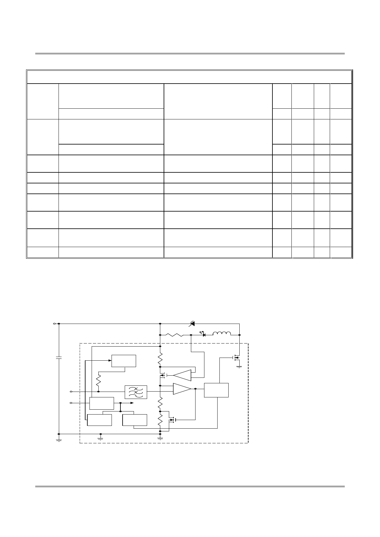
Block Diagram
V CC
V IN
RS
D1 LED
L1
LX
C1
4 .7 u F
ADJ
EN
GND
V ref.
R1
B uffer
R4
V o ltag e
reg u lato r
B and
gap
-
+
-
+
In tern al
R2
VDD
O ver
Tem p.
R3
MN
D riv er
TM Technology, Inc. reserves the right
P. 4
to change products or specifications without notice.
Publication Date:April 2014
Revision: E
Share Link: 