DK1401A-P Ver la hoja de datos (PDF) - PMD
Número de pieza
componentes Descripción
Fabricante
DK1401A-P Datasheet PDF : 70 Pages
| |||
Electrical Characteristics
Overview
The MC1401A-consists of two 68 pin PLCC's both fabricated in CMOS.
The Peripheral Input/Output IC (I/O chip) is responsible for interfacing
to the host processor and to the position input encoders. The Command
Processor IC (CP chip) is responsible for all host command, profile and
servo computations, as well as for outputting the PWM and DAC
signals.
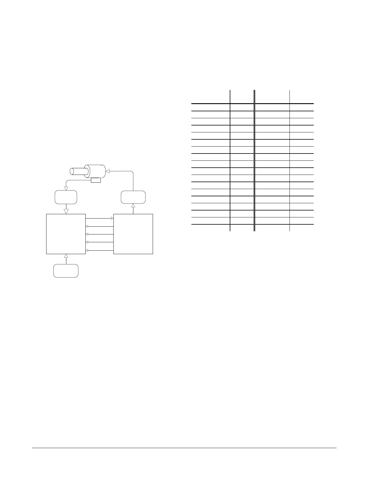
The following figure shows a typical system block diagram, along with
the pin connections between the I/O chip and the CP chip.
Motor
(4 axis)
Encoder
(1-4 axis)
Data4-11
I/OAddr0-3
I/O
I/OWrite
I/OCntrl0-3
ClkOut
Amplifier
(1-4 axis)
CP
Host
Processor
The CP and I/O chips function together as one integrated motion
processor. The major components connected to the chip set are the
Encoder (4, 2, or 1 axes), the motor amplifier (4, 2, or 1 axes), and the
host processor.
For the standard MC1401A parts (non '-P' parts), the encoder signals
are input to the I/O chip in quadrature format. For the '-P' parts the
encoder information is input directly into the CP chip, via an 8 bit data
bus and various control signals.
The chipset's motor output signals are connected to the motor amplifier.
Two types of output are provided; PWM (pulse width modulation), and
DAC-compatible signals used with an external DAC (digital to analog
converter).
The host processor is interfaced via an 8-bit bi-directional bus and
various control signals. Host communication is coordinated by a
ready/busy signal, which indicates when communication is allowed.
Interconnections between the two chips consist of a data bus and
various control and synchronization signals. The following table
summarizes the signals that must be interconnected for the chipset to
function properly. For each listed signal the I/O chip pin on the left side
of the table is directly connected to the pin to the right.
I/O Chip Signal
Name
CPData4
CPData5
CPData6
CPData7
CPData8
CPData9
CPData10
CPData11
CPAddr0
CPAddr1
CPAddr2
CPAddr3
CPCntr0
CPCntr1
CPCntr2
CPCntr3
CPWrite
CPClk
I/O Chip
Pin
18
5
6
7
8
17
3
1
68
27
29
12
20
36
22
63
2
46
CP Chip
Signal Name
Data4
Data5
Data6
Data7
Data8
Data8
Data10
Data11
I/OAddr0
I/OAddr1
I/OAddr2
I/OAddr3
I/OCntr0
I/OCntr1
I/OCntr2
I/OCntr3
I/OWrite
ClkOut
CP Chip
Pin
50
49
46
43
40
39
36
35
28
9
6
5
16
18
68
67
15
19
For a complete description of all pins see the 'Pin Descriptions'
section of this manual.
Unless specifically noted otherwise, the term 'MC1401A' refers to
the MC1401A, MC1201A, MC1101A, MC1401A-P, MC1201A-P, and
MC1101A-P Motion Processors.
Absolute Maximum Ratings
Unless otherwise stated, all electrical specifications are for both
the I/O and CP chips.
Storage Temperature, Ts.....................-55 deg. C to +150 deg. C
Supply Voltage, Vcc.............................-0.3 V to +7.0 V
Power Dissipation, Pd..........................650 mW (I/O and CP
combined)
Operating Ratings
Operating Temperature, Ta .................0 deg. C to +70 deg. C*
Nominal Clock Frequency, Fclk ...........25.0 Mhz
Supply Voltage, Vcc.............................4.75 V to 5.25 V
* Industrial and Military operating ranges also available. Contact your
PMD representative for more information.
4
Share Link: 