MC2800SYNEVK Ver la hoja de datos (PDF) - Motorola => Freescale
Número de pieza
componentes Descripción
Fabricante
MC2800SYNEVK Datasheet PDF : 11 Pages
| |||
FreescaleMCS2e80m0SicYoNnEVdKuctor, Inc.
APPLICATION NOTES
This frequency synthesized FLEX paging receiver board
uses Motorola’s NPN silicon low–noise high–frequency
transistors MMBR941LT1 to construct the RF functional
blocks, including a LNA, a voltage controlled oscillator
(VCO), a frequency multiplier and a mixer. NPC’s PLL IC
SM5166AV is used as the core of the fractional–N
synthesizer. The varactor diode MMBV609LT1 is used in the
VCO. The M–ary FSK IF receiver MC2800 performs the
second down–conversion and demodulates the received
FSK signal into two digital output bits for the baseband. Two
general purpose NPN & PNP BJTs, MMBT3904LT1 &
MMBT3906LT1 form the RSSI to RF AGC conversion circuit.
The LNA employs cascode architecture (Q1 and Q2) with
its output being matched to 230 , the input impedance of the
281–MHz SAW filter. The gain of the LNA is controlled by the
base voltage of Q2, which is a function of the RSSI output of
MC2800. The input matching network should be changed
when an antenna precedes the LNA. Special care must be
taken in characterizing the LNA and antenna to achieve a
good interface match.
The frequency synthesizer comprises a VCO, a NPC’s
PLL IC SM5166AV, a loop filter and a frequency multiplier.
The VCO (Q4) uses a modified Colpitts structure with a
varactor diode D2 for the frequency tuning. C52 can be
adjusted to change the frequency tuning range. The PLL
uses an input reference frequency of 20.950 MHz with a
divider value of 2514 (decimal), which results in a frequency
spacing of 8.333 kHz. The pre–scalar value of the PLL has a
control range from 10256 to 10576 (decimal). The loop filter
consisting of R26, R27, C64 & C65 has a bandwidth of about
1/10 to 1/15 of the frequency spacing. Q5 is used for
frequency multiplication with a ratio of 3. The third harmonic
is extracted by the bandpass filter formed by C16, C17, C62,
C63 & L11. This results in a synthesized frequency range
from 256.600 to 264.600 MHz. For the details of the control of
PLL IC, please refer to the data sheet of SM5166AV.
A common emitter circuit (Q3) is used as the mixer with
both LO and RF being ac–coupled to its base. Its output is
dc–coupled to the 21.4–MHz crystal filter. To minimize the
distortion of the downconverted frequency spectrum, the filter
output must be matched to MIX_IN of the MC2800.
For the characteristics of the MC2800 as well as its control
(ENABLE & RESET pins) and bit–rate filter (R1 pins) setup,
please refer to the MC2800 data sheet. It is recommended
that a single ceramic filter configuration be used. That is, a
450–kHz filter (FILTER3 in Figure 2) is inserted between the
MIX_OUT and IF1_IN, and a 1.0 F multi–layer ceramic chip
capacitor (C73 in Figure 2) is connected between the
IF1_OUT and IF2_IN. Although it is noted in the data sheet of
MC2800 that 3.0 to 4.0 dB performance degradation is
observed in the single ceramic filter application, this
performance degradation does not occur in the overall RF/IF
system performance. This is because the high gain and the
low NF of the RF front–end have effectively reduced the
noise contribution of the MC2800 to the overall system.
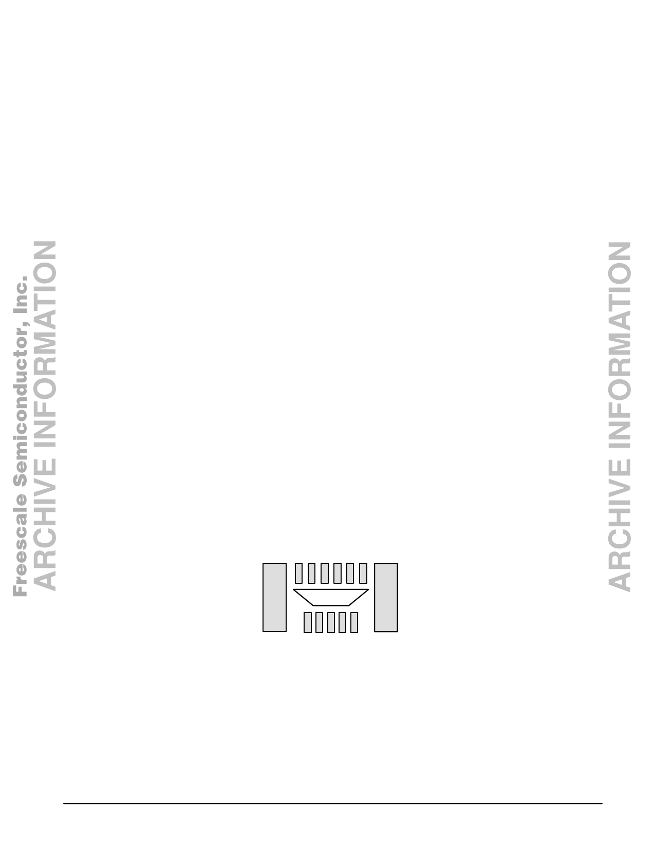
FDB Interface
This pager board uses an 11–pin surface mount socket to
interface with the pager baseband board. This interface
provides 2 digital output pins (D1 & D2), 6 control pins
(ENABLE, RESET, R1, PLL_DATA, PLL_CLOCK &
PLL_LATCH) and 3 supply pins (VCC, VDD & GND). The pin
descriptions are summarized in the following table and the
footprint of this socket is depicted in Figure 3. In order to
provide default states for these input pins, a pull up resistor
(R16) is used at R1 input pin whereas pull down resistors
(R17, R20, R21, R22 & R25) are connected at the rest of
input pins.
Note: For general information regarding FLEX products,
please contact the local Motorola SPS sales office or the web
at http://www.motorola.com/wireless–semi.
Figure 3. The Footprint of the 11 Pin Interface Socket
6 7 8 9 10 11
5 43 21
6
For More Information On This Product, MOTOROLA RF/IF DEVICE DATA
Go to: www.freescale.com
Share Link: 