EN5312QI Ver la hoja de datos (PDF) - Enpirion, Inc.
Número de pieza
componentes Descripción
Fabricante
EN5312QI Datasheet PDF : 16 Pages
| |||
March 2007
Pin Description
VIN
1
VIN
2
GND 3
GND 4
VOUT 5
VOUT 6
EN5312Q
16 VFB
15 VSENSE
14 NC
13 NC
12 NC
11 NC
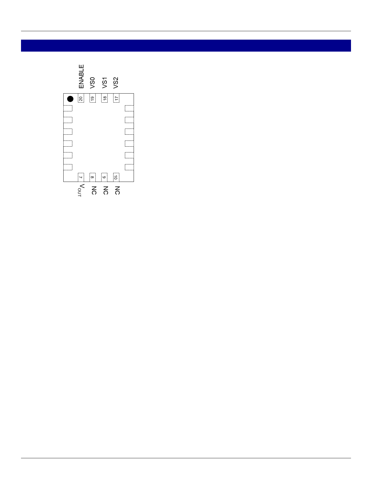
Figure 2. Pin description, top view.
VIN (Pin 1,2): Input voltage pin. Supplies power
to the IC. VIN can range from 2.4V to 5.5V.
Input GND: (Pin 3): Input power ground.
Connect this pin to the ground terminal of the
input capacitor.
Refer to
Layout
Recommendations for further details.
Output GND: (Pin 4): Power ground. The
output filter capacitor should be connected
between this pin and VOUT. Refer to Layout
recommendations for further detail.
VOUT (Pin 5,6,7): Regulated output voltage.
NC (Pin 8,9,10,11,12,13,14): These pins
should not be electrically connected to each
EN5312QI
other or to any external signal, voltage, or
ground. One or more of these pins may be
connected internally.
VSENSE (Pin 15): Sense pin for output voltage
regulation. Connect VSENSE to the output
voltage rail as close to the terminal of the
output filter capacitor as possible.
VFB (Pin 16): Feed back pin for external divider
option. When using the external divider option
(VS0=VS1=VS2= high) connect this pin to the
center of the external divider. Set the divider
such that VFB = 0.603V.
VS0,VS1,VS2 (Pin 17,18,19): Output voltage
select. VS0=pin19, VS1=pin18, VS2=pin17.
Selects one of seven preset output voltages or
choose external divider by connecting pins to
logic high or low. Logic low is defined as VLOW
≤ 0.4V. Logic high is defined as VHIGH ≥ 1.4V.
Any level between these two values is
indeterminate.
ENABLE (Pin 20): Output enable. Enable =
logic high, disable = logic low. Logic low is
defined as VLOW ≤ 0.2V. Logic high is defined
as VHIGH ≥ 1.4V. Any level between these two
values is indeterminate.
Bottom Thermal Pad: Device thermal pad to
remove heat from package. Connect to PCB
surface ground pad and PCB internal ground
plane (see layout recommendations).
©Enpirion 2007 all rights reserved, E&OE
2
www.enpirion.com
Share Link: 