MAX820 Ver la hoja de datos (PDF) - Maxim Integrated
Número de pieza
componentes Descripción
Fabricante
MAX820 Datasheet PDF : 16 Pages
| |||
Microprocessor and Nonvolatile
Memory Supervisory Circuits
MR
RESET
25µs MIN
12µs TYP
VIN
3
VCC
4 RESET IN/INT
RESET 2
TO µP
CE IN OV
CE OUT
15µs TYP
MAX792
5 LLIN/REFOUT
RESET 1
TO µP
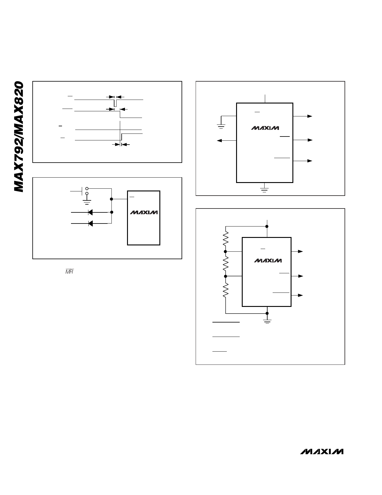
Figure 2. Manual-Reset Timing Diagram
MANUAL RESET
OTHER
RESET
SOURCES
9
MR
*
*
...
MAX792
MAX820
* DIODES NOT REQUIRED ON OPEN-DRAIN OUTPUTS
Figure 3. Diode "OR" connections allow multiple reset sources
to connect to MR.
Low-Line Output
In internal threshold mode, the low-line comparator
monitors VCC with a threshold voltage typically 120mV
above the reset threshold, and with 15mV of hysteresis.
For normal operation (VCC above the reset threshold),
LOWLINE is pulled to VCC. Use LOWLINE to provide an NMI
to the µP, as described in the previous section, when
VCC begins to fall (Figure 4).
Reset Function
The MAX792/MAX820 provide both RESET and RESET
outputs. The RESET and RESET outputs ensure that the
µP powers up in a known state, and prevent code-exe-
cution errors during power-up, power-down, or
brownout conditions.
The reset function will be asserted during the following
conditions:
1) VCC less than the programmed reset threshold.
2) MR less than 1.30V typ.
3) Reset remains asserted for 200ms typ after VCC
rises above the reset threshold or after MR has
exceeded 1.30V typ.
LOW LINE 10
TO µP NMI
GND
12
Figure 4a. Connection for Internal Threshold Mode
VIN
3
R1
VCC
RESET IN/INT
RESET 2 TO µP
R2
MAX792
LLIN/REFOUT
RESET 1 TO µP
R3
R3 = 1.30V x VCC MAX
VLOW LINE x IMAX
R2 = 1.30V x VCC MAX – R3
VRESET x IMAX
R1 =
VCC MAX
IMAX
– (R2 + R3)
10
LOW LINE
GND
12
TO µP NMI
IMAX = THE MAXIMUM DESIRED CURRENT
THROUGH THE VOLTAGE DIVIDED.
Figure 4b. Connection for External Threshold Programming Mode
When reset is asserted, all the internal counters are
reset, the watchdog output (WDO) and watchdog-pulse
output (WDPO) are set high, and the set watchdog-time-
out input (SWT) is set to (VCC - 0.6V) if it is not already
connected to VCC (for internal timeouts). The chip-
enable transmission gate is also disabled while reset is
asserted; the chip-enable input (CE IN) becomes high
impedance and the chip-enable output (CE OUT) is
pulled up to VCC.
10 ______________________________________________________________________________________
Share Link: 