MSK3017 Ver la hoja de datos (PDF) - M.S. Kennedy
Número de pieza
componentes Descripción
Fabricante
MSK3017 Datasheet PDF : 5 Pages
| |||
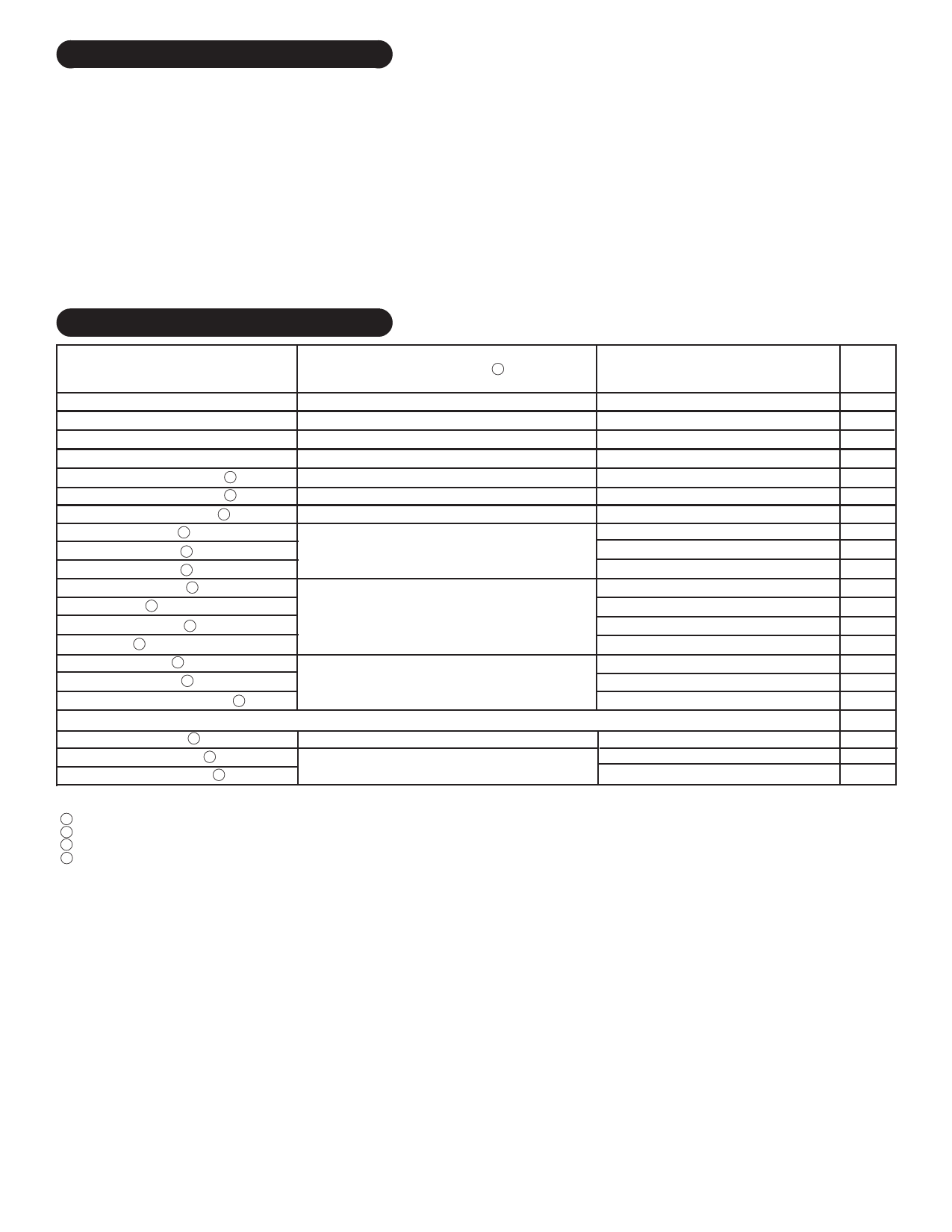
ABSOLUTE MAXIMUM RATINGS
VDSS
VDGDR
VGS
ID
IDM
RTH-JC
RTH-JC
Drain to Source Voltage ○ ○ ○ ○ 200V MAX
Drain to Gate Voltage
(R =1MΩ) 200V MAX GS
○
○
○
○
○
○
○
○
○
○
○
Gate to Source Voltage
(Continuous)
±20V MAX ○
○
○
○
○
○
○
○
○
○
Continuous Current ○ ○ ○ ○ ○ ○ ○ 30A MAX
Pulsed Current ○ ○ ○ ○ ○ ○ ○ ○ ○ ○ 46A MAX
Thermal Resistance
(Junction to Case)@25°C ○ ○ ○ ○ ○ 1.0°C/W
Thermal Resistance
(Junction to Case)@125°C ○ ○ ○ ○ 1.6°C/W
Single Pulse Avalanche Energy
○
○
○
○
○
○
○
○
○1000 mJ
TJ Junction Temperature
+150°C MAX
○
○
○
○
○
○
○
○
○
○
○
TST Storage Temperature ○ ○ ○ ○ ○ ○ ○ ○ ○ -55°C to +150°C
TC Case Operating Temperature Range -55°C to +125°C
TLD Lead Temperature Range
(10 Seconds Lead Only) ○ ○ ○ ○ ○ ○ ○ ○ ○ ○ ○ 200°C MAX
ELECTRICAL SPECIFICATIONS
Parameter
Test Conditions 4
Min.
MSK3017
Typ.
Max.
Units
Drain-Source Breakdown Voltage
VGS=0 ID=0.25mA
200
-
-
V
Drain-Source Leakage Current
VDS=200V VGS=0V
-
-
250
μA
Gate-Source Leakage Current
VGS=±20V VDS=0
-
-
±100
nA
Gate-Source Threshold Voltage
VDS=VGS ID=250μA
2.0
-
4.0
V
Drain-Source On Resistance 2
VGS=10V ID = 30A
-
-
0.09
Ω
Drain-Source On Resistance 3
VGS=10V ID=30A
-
-
0.06
Ω
Forward Transconductance 1
VDS=50V ID=30A
24
-
-
S
Total Gate Charge 1
ID = 30A
-
-
230
nC
Gate-Source Charge 1
VDS=160V
-
-
42
nC
Gate-Drain Charge 1
Turn-On Delay Time 1
VGS = 10V
VDD=100V
-
-
110
nC
-
23
-
nS
Rise Time 1
ID = 30A
-
120
-
nS
Turn-Off Delay Time 1
RG = 4.3Ω
-
100
-
nS
Fall Time 1
RD = 2.1Ω
-
94
-
nS
Input Capacitance 1
Output Capacitance 1
VGS=0V
VDS=25V
-
5200
-
pF
-
1200
-
pF
Reverse Transfer Capacitance 1
f=1MHz
-
310
-
pF
Body Diode
Forward On Voltage 1
IS=30 A VGS=0V
-
1.8
-
V
Reverse Recovery Time 1
IS=30 A di/dt=100A/μS
-
390
590
nS
Reverse Recovery Charge 1
-
4.8
7.2
μC
NOTES:
1 This parameter is guaranteed by design but need not be tested. Typical parameters are representative of actual device performance but are for reference only.
2 Resistance as seen at package pins.
3 Resistance for die only; use for thermal calculations.
4 TA=25°C unless otherwise specified.
2
Rev. A 7/10
Share Link: 