MSK5150 Ver la hoja de datos (PDF) - M.S. Kennedy
Número de pieza
componentes Descripción
Fabricante
MSK5150 Datasheet PDF : 5 Pages
| |||
APPLICATION NOTES
REGULATOR PROTECTION:
The MSK 5150 series is fully protected against reversed input
polarity, overcurrent faults, overtemperature conditions (Pd) and
transient voltage spikes of up to 60V. If the regulator is used
in dual supply systems where the load is returned to a negative
supply, the output voltage must be diode clamped to ground.
OUTPUT CAPACITOR:
The output voltage ripple of the MSK 5150 series voltage regu-
lators can be minimized by placing a filter capacitor from the
output to ground. The optimum value for this capacitor may
vary from one application to the next, but a minimum of 20µF
is recommended for optimum performance. This capacitor need
not be an expensive low ESR type: aluminum electrolytics are
adequate. In fact, extremely low ESR capacitors may contrib-
ute to instability. Tantalum capacitors are recommended for
systems where fast load transient response is important. Tran-
sient load response can also be improved by placing a capaci-
tor directly across the load.
LOAD CONNECTIONS:
In voltage regulator applications where very large load cur-
rents are present, the load connection is very important. The
path connecting the output of the regulator to the load must be
extremely low impedance to avoid affecting the load regulation
specifications. Any impedance in this path will form a voltage
divider with the load. The MSK 5150 series requires a mini-
mum of 10mA of load current to stay in regulation.
ENABLE PIN:
The MSK 5150 series of voltage regulators are equipped with a
TTL compatible ENABLE pin. A TTL high level on this pin acti-
vates the internal bias circuit and powers up the device. A TTL
low level on this pin places the controller in shutdown mode
and the device draws approximately 10µA of quiescent current.
If the enable function is not used, simply connect the enable pin
to the input.
FLAG OUTPUT PIN:
All of the fixed output voltage versions of the MSK 5150 series
are equipped with a flag output pin. Since the flag pin is an
open collector configuration it can be pulled up to any voltage
between 3V and 26V. This feature allows direct interfacing to
practically any logic. This active low output has a typical level
of 0.22V when the flag comparator detects an "out of regula-
tion" condition. Flag states include low input voltage, out of
regulation and output current limit. Extremely high level input
voltage transients will also cause the flag output pin to acti-
vate.
HEAT SINK SELECTION:
To select a heat sink for the MSK 5150, the following formula
for convective heat flow may be used.
Governing Equation:
Tj = Pd x (Rθjc + Rθcs + Rθsa) + Ta
WHERE:
Tj = Junction Temperature
Pd = Total Power Dissipation
Rθjc = Junction to Case Thermal Resistance
Rθcs = Case to Heat Sink Thermal Resistance
Rθsa = Heat Sink to Ambient Thermal Resistance
Ta = Ambient Temperature
First, the power dissipation must be calculated as follows:
Power Dissipation = (Vin - Vout) x Iout
Next, the user must select a maximum junction temperature.
The absolute maximum allowable junction temperature is 125°C.
The equation may now be rearranged to solve for the required
heat sink to ambient thermal resistance (Rθsa).
EXAMPLE:
An MSK 5150-3.3 is configured for Vin=+5V and
Vout=+3.3V. Iout is a continuous 1A DC level. The ambient
temperature is +25°C. The maximum desired junction tem-
perature is 125°C.
Rθjc = 1.5°C/W and Rθcs = 0.15°C/W for most thermal greases
Power Dissipation= (5V - 3.3V) x (1A)
= 1.7 Watts
Solve for Rθsa:
Rθsa = 125°C - 25°C - 1.5°C/W - 0.15°C/W
1.7W
= 57.17°C/W
In this example, a heat sink with a thermal resistance of no
more than 57°C/W must be used to maintain a junction tem-
perature of no more than 125°C.
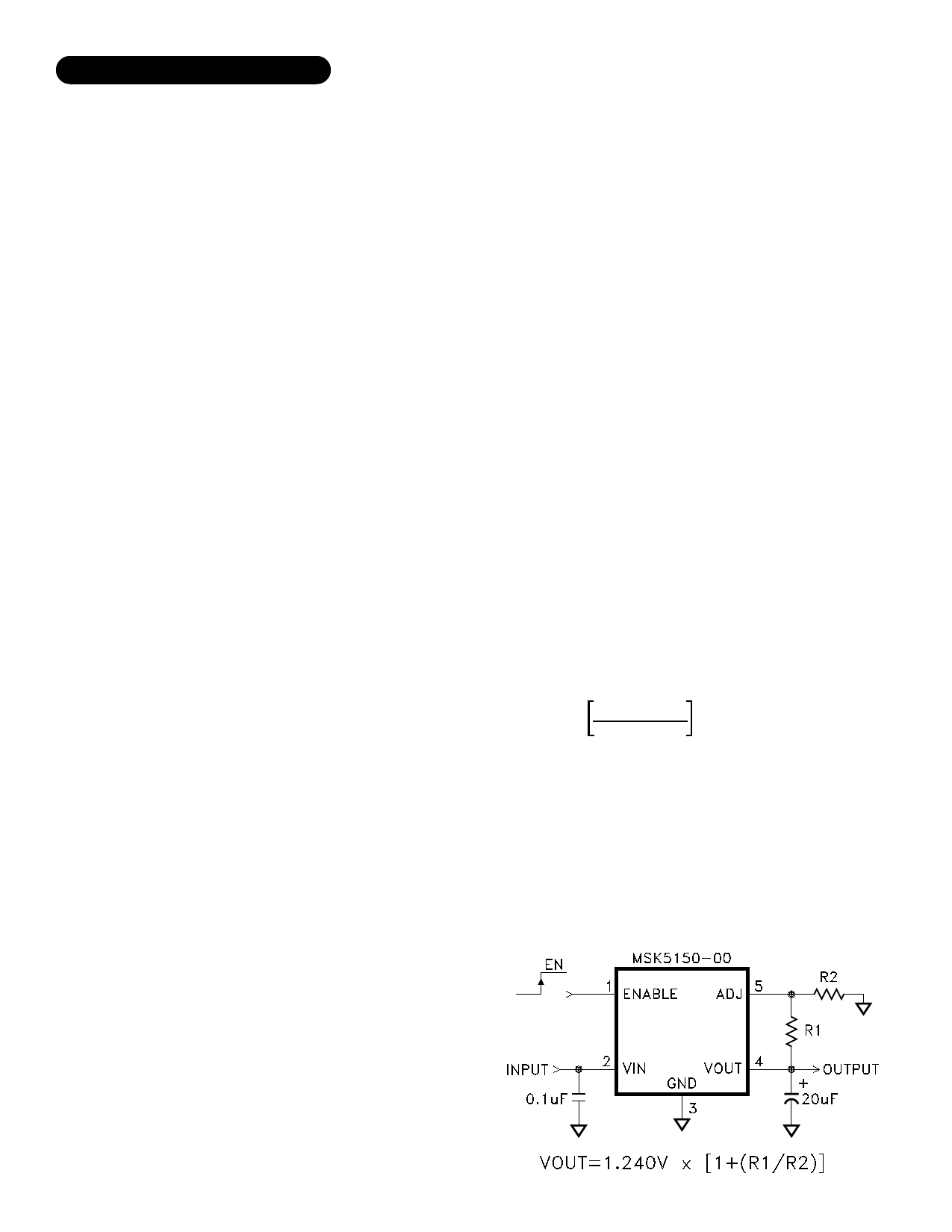
MSK5150-00 OUTPUT ADJUSTMENT:
The MSK 5150-00 is an adjustable version in the series of high
performance regulators. The diagram below illustrates proper
adjustment technique for the output voltage. The series resis-
tance of R1+R2 should be selected to pass the minimum regu-
lator output current requirement of 10mA.
DEVICE/CASE CONNECTION:
The MSK 5150 series are highly thermally conductive devices
and the thermal path from the package heat sink to the internal
junctions is very short. Since the case is electrically isolated
from the internal circuitry, the package can be directly con-
nected to a heat sink.
3
Rev. F 1/06
Share Link: 