MSK130 Ver la hoja de datos (PDF) - Anaren Microwave
Número de pieza
componentes Descripción
Fabricante
MSK130 Datasheet PDF : 6 Pages
| |||
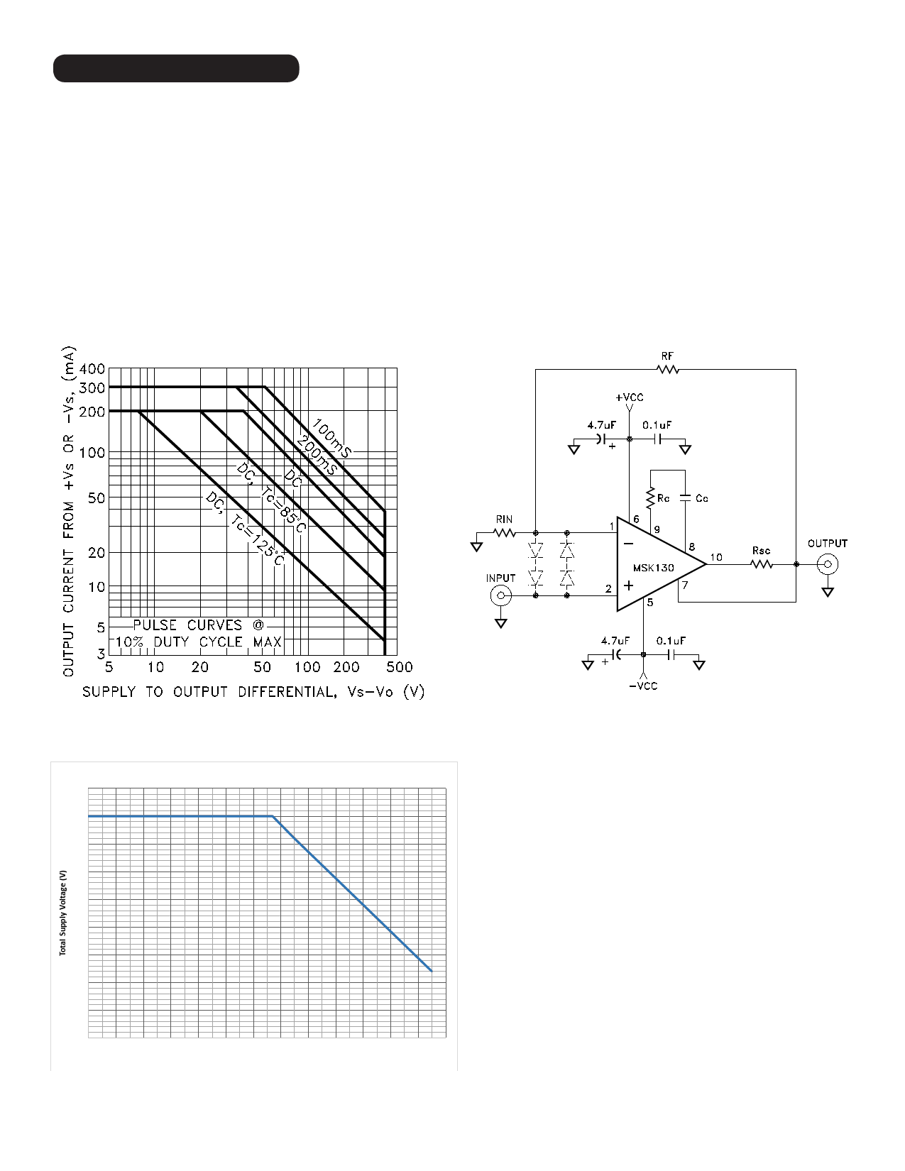
APPLICATION NOTES
SAFE OPERATING AREA
The output stage of the MSK130 is fabricated using state of the
art complimentary MOSFETs and is free from secondary breakdown
limitations. There are two distinct limitations for the output stage:
1. The internal wire bonds and the geometry of the MOSFET have
a maximum peak current capability of ±300mA.
2. The junction temperature of each MOSFET should be kept below
the maximum rating of 150°C.
The SOA Curves below illustrate various conditions of power
dissipation.
INPUT PROTECTION
The MSK130 can safely handle up to ±25V of differential input
voltages. In applications where this may be violated, external
protection is required. Four diodes can be used as shown in the
typical connection diagram. If leakage current is of concern, use
JFETs connected as diodes instead. JFETs will also yield very low
capacitance for high speed applications.
CURRENT LIMIT
The MSK130 has an internal active current limit circuit that can
be programmed with a single external resistor Rsc. The value of
this resistor should be kept between 2Ω and 150Ω. The following
equation is used to select the resistor for a given current limit value:
Rsc = 0.6/ILIMIT (See Typical Connection Diagram)
TYPICAL CONNECTION DIAGRAM
STABILITY AND COMPENSATION
Safe Operating Area - Suppy Voltage vs. Temperature
450
400
350
300
250
Since the MSK130 is externally compensated the bandwidth
can be optimized for any gain selection. The external compensation
components should be located as close to the compensation pins
as possible to avoid unwanted oscillations. The capacitor Cc
should be rated for the full supply voltage. Use a high quality
dielectric such as NPO to maintain a desired compensation over
the full operating temperature. Refer to the typical performance
curves for a guide to select the desired compensation. Refer to
the typical connection diagram for the location of the Rc and Cc
components.
200
POWER SUPPLIES
150
Both the negative and positive power supplies must be
100
effectively decoupled with a high and low frequency bypass circuit
to avoid power supply induced oscillation. An effective decoupling
50
scheme consists of a 0.1 microfarad ceramic capacitor in parallel
0
with a 4.7 microfarad tantalum capacitor for each power supply
0 10 20 30 40 50 60 70 80 90 100 110 120 130 pin to ground. All power supply decoupling capacitors should be
Baseplate Temperature (deg C)
placed as close to the package power supply pins as possible
(pins 5 and 6).
3
8548-125 Rev. F 1/18
Share Link: 