MC141519T Ver la hoja de datos (PDF) - Motorola => Freescale
Número de pieza
componentes Descripción
Fabricante
MC141519T Datasheet PDF : 14 Pages
| |||
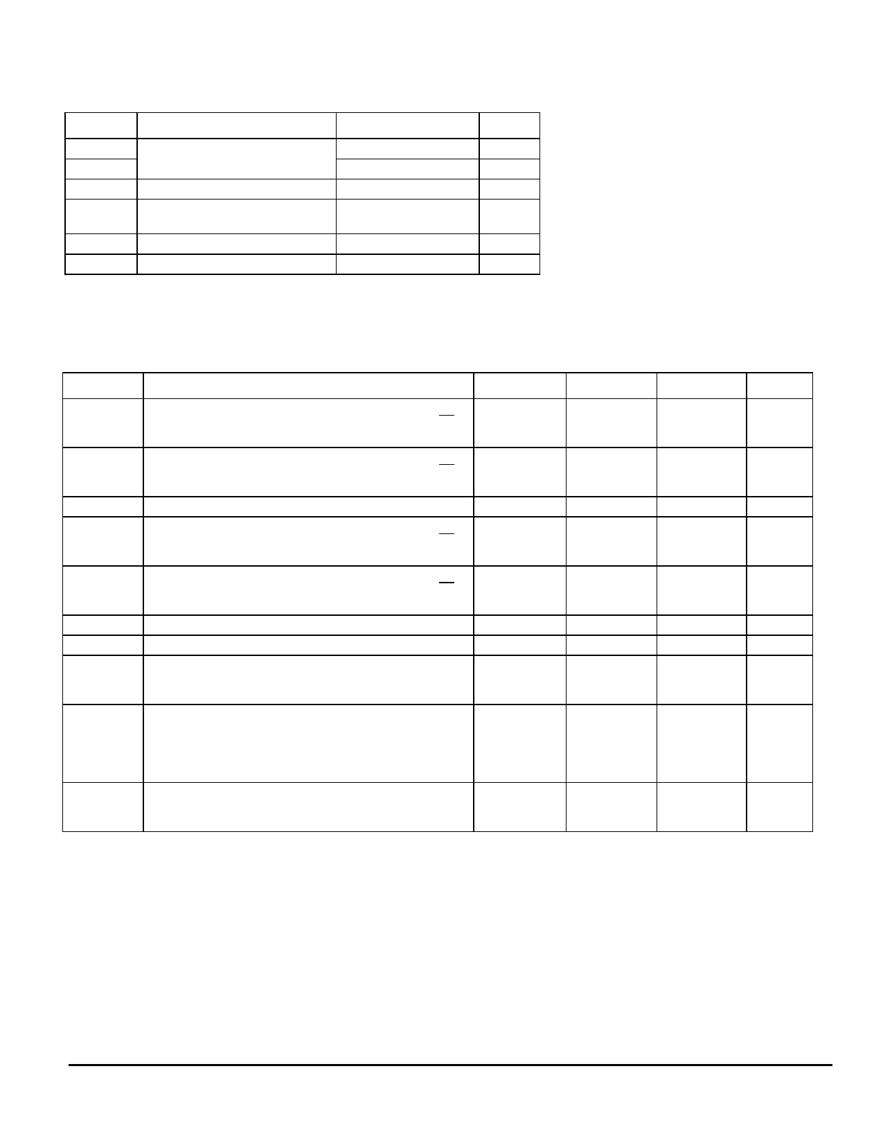
MAXIMUM RATINGS* (Voltages Referenced to VSS, TA = 25˚C)
Symbol
Parameter
Value
Unit
VDD
Supply Voltage
-0.3 to +7.0
V
V<1>
VSS-0.3 to VSS+22.0
V
Vin
Input Voltage
VSS-0.3 to VDD+0.3
V
I
Current Drain Per Pin Excluding VDD
25
mA
and VSS
TA
Operating Temperature Range
-20 to 80
˚C
Tstg
Storage Temperature Range
-65 to +150
˚C
* Maximum Ratings are those values beyond which damage to the device may occur. Func-
tional operation should be restricted to the limits in the Electrical Characteristics tables or Pin
Description section.
ELECTRICAL CHARACTERISTICS (Voltages Referenced to VSS, TA = 25˚C, VDD = 5.0V)
Symbol
Parameter
Min
VIH
VIL
VR
Iin
Cin
VOH
VOL
VDD
V<1>
IACC
IDP
ISB
ILDP
ILSB
Input High Voltage
BPCLK, FRM,P02,RAA,CR1,CR2,BS,
D6-D0,SD1,SD2,SHCLK,DOFF,M,DIRR
Input Low Voltage
BPCLK, FRM,P02,RAA,CR1,CR2,BS,
D6-D0,SD1,SD2,SHCLK,DOFF,M,DIRR
Data Retention
Input Current
BPCLK, FRM,P02,RAA,CR1,CR2,BS,
D6-D0,SD1,SD2,SHCLK,DOFF,M,DIRR
Capacitance
BPCLK, FRM,P02,RAA,CR1,CR2,BS,
D6-D0,SD1,SD2,SHCLK,DOFF,M,DIRR
Output High Voltage
SD1,SD2
Output Low Voltage
SD1,SD2
Operating Voltages
Supply Voltage (referenced to VSS)
LCD Voltage (referenced to VSS)
Operating supply current
VSS)
Access Mode
Display Mode
Standby Mode
(VDD)(VDD=5V, referenced to
Operating supply current (V<1>)(V<1>=20V, referenced to VSS)
Display Mode
Standby Mode
0.7xVDD
VSS
2.0
-
-
0.8xVDD
VSS
2.7
8.0
-
-
-
-
-
This device contains circuitry to protect the
inputs against damage due to high static volt-
ages or electric fields; however, it is advised that
normal precautions to be taken to avoid applica-
tion of any voltage higher than maximum rated
voltages to this high impedance circuit. For
proper operation it is recommended that Vin and
Vout be constrained to the range VSS < or = (Vin
or Vout) < or = VDD. Reliability of operation is
enhanced if unused input are connected to an
appropriate logic voltage level (e.g., either VSS or
VDD). Unused outputs must be left open. This
device may be light sensitive. Caution should be
taken to avoid exposure of this device to any light
source during normal operation. This device is
not radiation protected.
Typ
Max
Unit
-
VDD
V
-
0.3xVDD
V
-
-
V
-
1
uA
-
8
pF
-
VDD
V
-
0.2xVDD
V
-
5.5
V
-
20.0
V
150
200
uA
30
100
uA
1
10
uA
12
20
uA
1
10
uA
MC141519
3–98
MOTOROLA
Share Link: 