MPC9600AE Ver la hoja de datos (PDF) - Integrated Device Technology
Número de pieza
componentes Descripción
Fabricante
MPC9600AE Datasheet PDF : 15 Pages
| |||
MPC9600 Data Sheet
LOW VOLTAGE, 2.5V AND 3.3V LVCMOS PLL CLOCK DRIVER
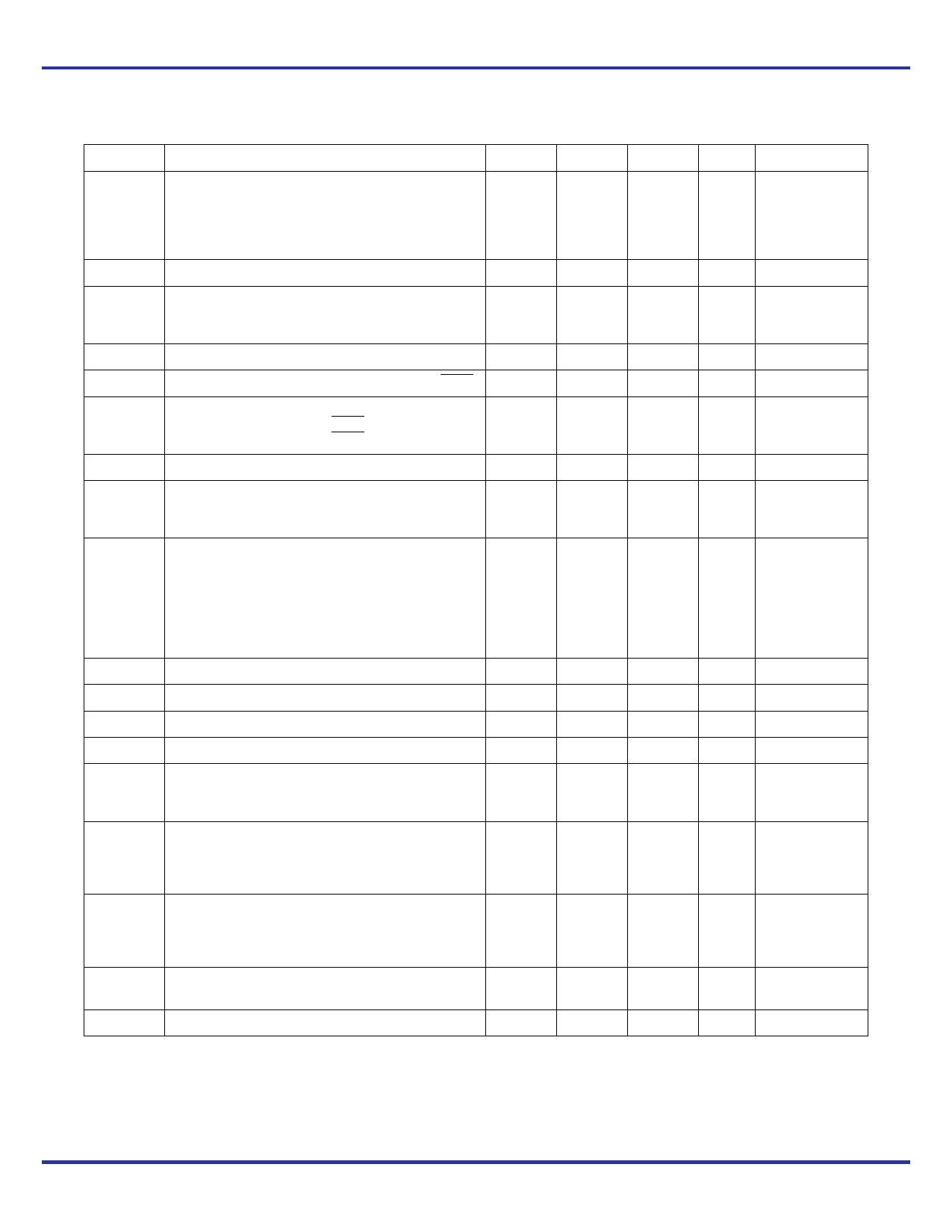
Table 7. AC Characteristics – 48 LQFP (VCC = 3.3 V ± 5% or VCC = 2.5 V ± 5%, TA = –40°C to +85°C)(1)
Symbol
Characteristics
Min
Typ
Max
Unit
fref
Input Frequency
8 feedback (FSEL_FB = 0)
12 feedback (FSEL_FB = 1)
25
16.67
50
MHz
33
MHz
Condition
PLL locked
PLL locked
Static test mode (VCCA = GND)
0
fVCO
VCO Frequency
200
fMAX
Maximum Output Frequency
2 outputs (FSELx = 0)
100
4 outputs (FSELx = 1)
50
500
MHz VCCA = GND
400
MHz
200
MHz PLL locked
100
MHz PLL locked
frefDC
Reference Input Duty Cycle
25
VPP
Peak-to-Peak Input Voltage
PCLK, PCLK
500
VCMR(2) Common Mode Range
PCLK, PCLK (VCC = 3.3 V 5%)
1.2
PCLK, PCLK (VCC = 2.5 V 5%)
1.2
tr, tf
CCLK Input Rise/Fall Time
t()
Propagation Delay (static phase offset)
CCLK to FB_IN
–60
PECL_CLK to FB_IN
+30
75
1000
%
mV LVPECL
VCC –0.8
VCC –0.6
1.0
V LVPECL
V LVPECL
ns see Figure 11
+40
+130
+140
+230
ps PLL locked
ps PLL locked
tsk(o)
Output-to-Output Skew
all outputs, single frequency
all outputs, multiple frequency
within QAx output bank
within QBx outputs
within QCx outputs
70
150
ps Measured at
70
150
ps coincident rising
edge
30
75
ps
40
125
ps
30
75
ps
DC
Output Duty Cycle
45
50
55
%
tr, tf
Output Rise/Fall Time
0.1
1.0
ns see Figure 11
tPLZ, HZ Output Disable Time
10
ns
tPZL, ZH Output Enable Time
10
ns
BW
PLL Closed Loop Bandwidth
8 feedback (FSEL_FB=0)
12 feedback (FSEL_FB=1)
1.0 – 10
0.6 – 4.0
MHz
MHz
–3 dB point of PLL
transfer
characteristic
tJIT(CC)
Cycle-to-Cycle Jitter(3)
All outputs in 2 configuration
All outputs in 4 configuration
Refer to
application
40
130
ps section for other
40
180
ps configurations
tJIT(PER) Period Jitter(3)
All outputs in 2 configuration
All outputs in 4 configuration
Refer to
25
70
ps application
20
100
ps section for other
configurations
tJIT()
I/O Phase Jitter (1 )
VCC = 3.3 V
VCC = 2.5 V
17(4)
15(3)
ps RMS value at
ps fVCO = 400 MHz
tLOCK
Maximum PLL Lock Time
5.0
ms
1. AC characteristics are applicable over the entire ambient temperature and supply voltage range and are production tested. AC
characteristics apply for parallel output termination of 50 to VTT.
2. VCMR (AC) is the crosspoint of the differential input signal. Normal AC operation is obtained when the crosspoint is within the VCMR range
and the input swing lies within the VPP (AC) specification. Violation of VCMR or VPP impacts static phase offset t().
3. Cycle-to-cycle and period jitter depends on output divider configuration.
4. See Applications Information section for max I/O phase jitter versus frequency.
MPC9600 REVISION 6 JANUARY 7, 2013
6
©2013 Integrated Device Technology, Inc.
Share Link: 