HMC8142 Ver la hoja de datos (PDF) - Analog Devices
Número de pieza
componentes Descripción
Fabricante
HMC8142 Datasheet PDF : 16 Pages
| |||
Data Sheet
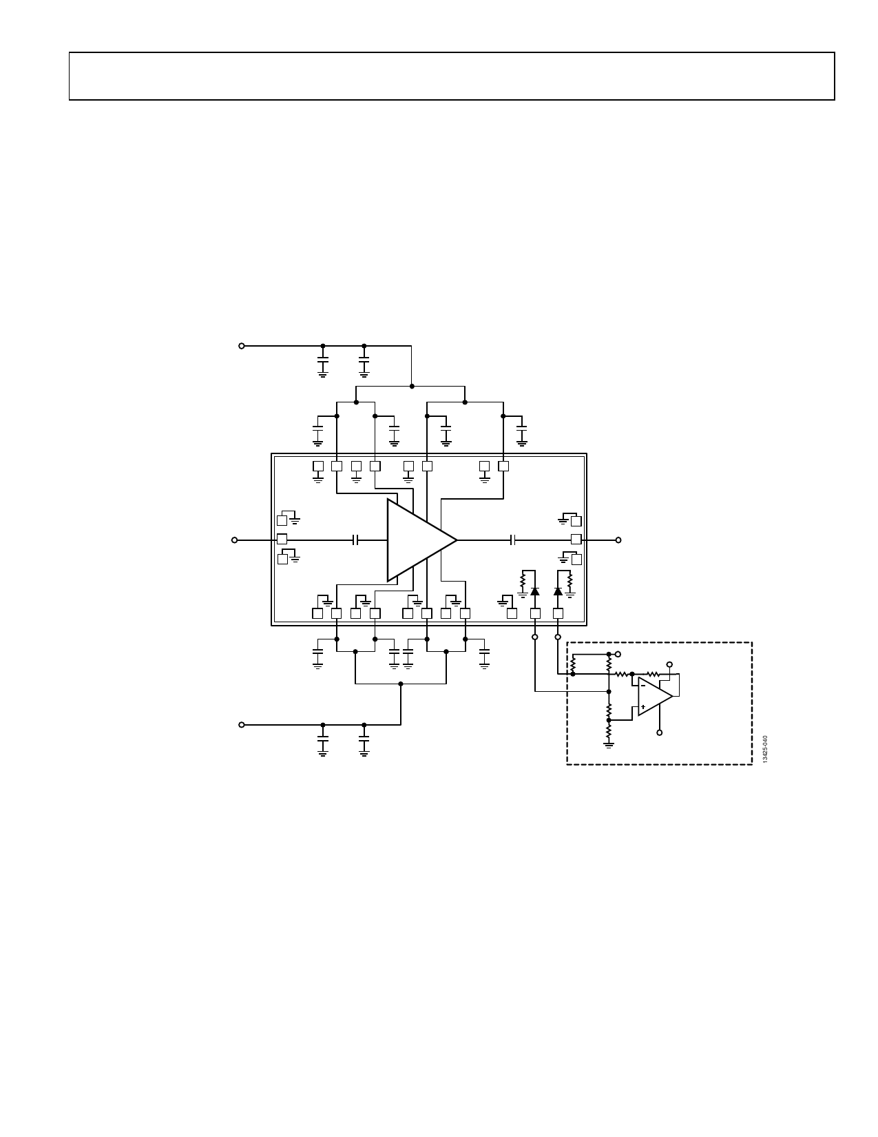
APPLICATIONS INFORMATION
TYPICAL APPLICATION CIRCUIT
A typical application circuit for the HMC8142 is shown in
Figure 40. Combine supply lines as shown in the application
circuit schematic to minimize external component count and
simplify power supply routing.
The HMC8142 uses several amplifier, detector, and attenuator
stages. All stages use depletion mode pHEMT transistors. It is
important to follow the following power-up bias sequence to
ensure transistor damage does not occur.
VDD1, VDD2, VDD3, VDD4
4.7µF
0.01µF
HMC8142
1. Apply a −2 V bias to the VGG1 to VGG4 pads.
2. Apply 4 V to the VDD1 to VDD4 pads.
3. Adjust VGG1 to VGG4 between −2 V and 0 V to achieve a
total amplifier drain current of 450 mA.
To power down the HMC8142, follow the procedure in reverse.
For additional guidance on general bias sequencing, see the
MMIC Amplifier Biasing Procedure application note.
RFIN
VGG1, VGG2, VGG3, VGG4
120pF
120pF
120pF
120pF
45 67
89
VDD1
VDD2
VDD3
10 11
VDD4
3
2
RFIN
1
12
RFOUT 13
14
VGG1
VGG2
VGG3
VGG4
25 24 23 22
21 20 19 18
VREF VDET
17 16 15
RFOUT
120pF
4.7µF
120pF
120pF 120pF
0.01µF
Figure 40. Typical Application Circuit
+5V
+5V
100kΩ 100kΩ 10kΩ
10kΩ
10kΩ
VOUT = VREF – VDET
10kΩ
–5V
SUGGESTED INTERFACE CIRCUIT
Rev. A | Page 13 of 16
Share Link: 