DTD113ZS Ver la hoja de datos (PDF) - ROHM Semiconductor
Número de pieza
componentes Descripción
Fabricante
DTD113ZS Datasheet PDF : 4 Pages
| |||
Transistors
DTD113ZK / DTD113ZU / DTD113ZS
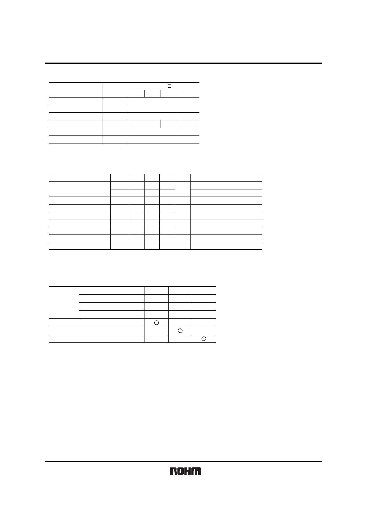
zAbsolute maximum ratings (Ta=25°C)
Parameter
Limits(DTD113Z )
Symbol
Unit
U
K
S
Supply voltage
VCC
50
V
Input voltage
VIN
−5 to +10
V
Output current
IC
500
mA
Power dissipation
Pd
200
300 mW
Junction temperature
Tj
150
°C
Storage temperature
Tstg
−55 to +150
°C
zElectrical characteristics (Ta=25°C)
Parameter
Symbol Min.
Input voltage
VI(off)
−
VI(on)
1.5
Output voltage
VO(on)
−
Input current
II
−
Output current
IO(off)
−
DC current gain
GI
82
Input resistance
R1
0.7
Resistance ratio
R2/R1
8
Transition frequency
fT
−
∗ Transition frequency of the device
Typ.
−
−
0.1
−
−
−
1
10
200
Max.
0.3
−
0.3
7.2
0.5
−
1.3
12
−
Unit
V
V
mA
µA
−
kΩ
−
MHz
Conditions
VCC=5V, IO=100µA
VO=0.3V, IO=20mA
IO/II=50mA/2.5mA
VI=5V
VCC=50V, V=0V
VO=5V, IO=50mA
−
−
VCE=10V, IE=−50mA, f=100MHz ∗
zPackaging specifications
Package
Packaging type
Code
Part No. Basic ordering unit (pieces)
DTD113ZK
DTD113ZU
DTD113ZS
SMT3
Taping
T146
3000
−
−
UMT3
Taping
T106
3000
−
−
SPT
Taping
TP
5000
−
−
Rev.A
2/3
Share Link: 