M62353AGP Ver la hoja de datos (PDF) - MITSUBISHI ELECTRIC
Número de pieza
componentes Descripción
Fabricante
M62353AGP Datasheet PDF : 6 Pages
| |||
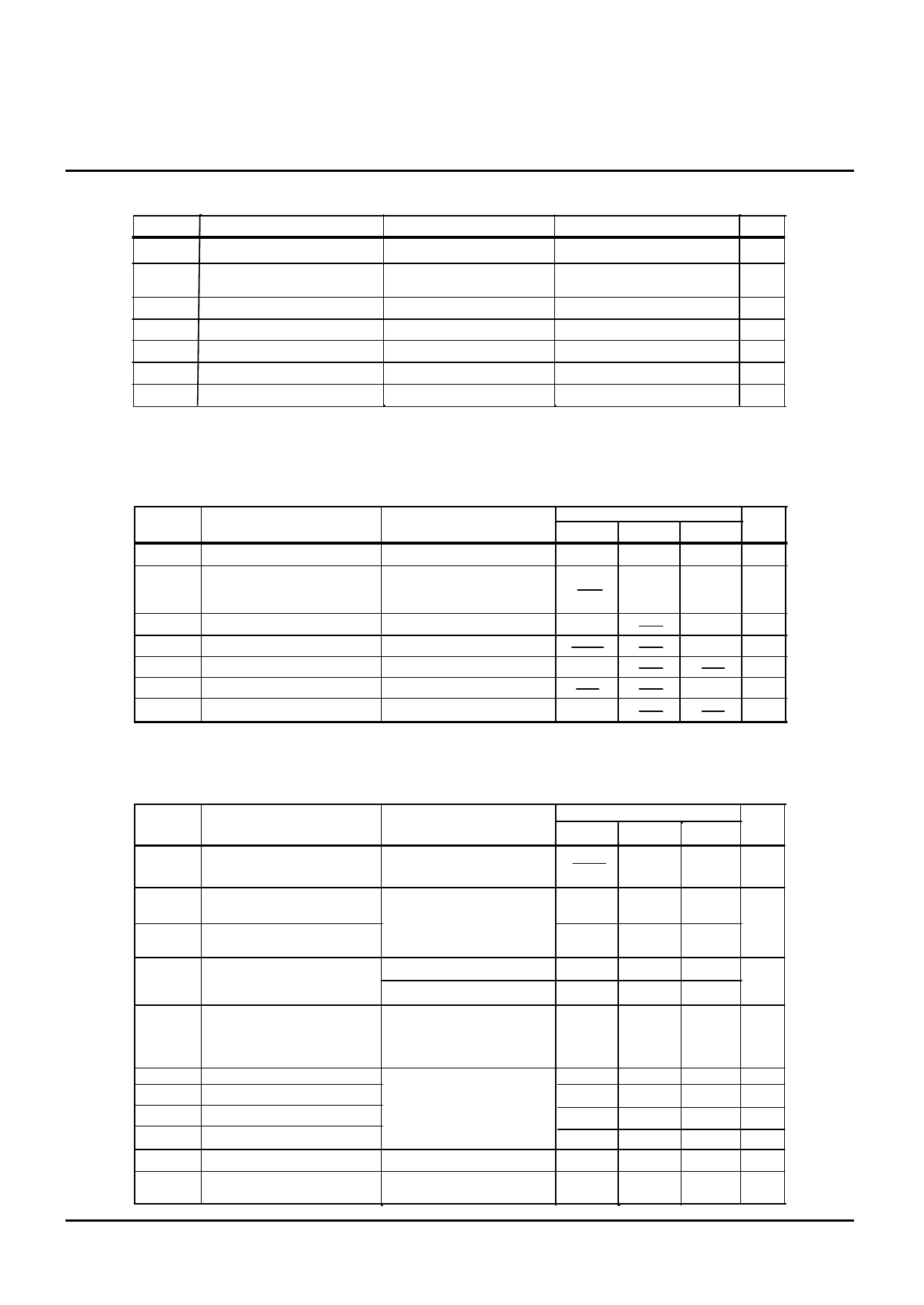
ABSOLUTE MAXMUM RATING
Symbol
Vcc
VDD
VIN
Vout
Pd
Topr
Tstg
Parameter
Supply voltage
D-A converter High
levelreference voltage
Digital input voltage
Output voltage
Power dissipation
Operating temperature
Storage temperature
MITSUBISHI <Standard Linear IC>
M62353AGP
8BIT 8CH D-A CONVERTER WITH BUFFER AMPLIFIERS
Conditions
Ratings
Unit
- 0.3 ~ 7.0
V
- 0.3 ~ 7.0
V
- 0.3 ~ V CC +0.3
V
- 0.3 ~ V CC +0.3
V
150
mW
- 20 ~ 85
°C
- 40 ~ 125
°C
ELECTRIC CHARACTERISTICS
<Digital part> (VCC, VrefU=5V ± 10% , VCC≥ VrefU, GND, VrefL=0.0V, Ta=-20 ~ + 85ºCunless otherwise specified.)
Symbol
Parameter
Vcc
Supply voltage
Conditions
Ratings
MIN
TYP
MAX Unit
4.5
5.0
5.5
V
Icc
Supply current
CLK=1MHz Operation
V CC =5V, IAO =0 A
1.0
2.5
mA
IILK
VIL
VIH
VOL
VOH
Input leak current
Digital input Low voltage
Digital input High voltage
Digital output Low voltage
Digital output High voltage
VIN =0 ~ V CC
IOL = 2.5mA
IOH = - 400 A
-10
2.0
VCC -0.4
Note2: Typical value is for Ta=25ºC
Note3: Changes from M62353GP: Digital input voltage corresponds to TTL spec.
10
A
0.8
V
V
0.4
V
V
<Analog Part> (VCC, VrefU=5V ± 10% , VCC≥ VrefU, GND, VrefL=0.0V, Ta=-20 ~ + 85ºCunless otherwise specified.)
Symbol
Parameter
IrefU
Reference voltage
pin current
D-A converter High level
VDD (V refU )
reference voltage range
D-A converter Low level
VSS (V refL )
reference voltage range
Buffer amplifier
VAO
output drive range
IAO
Buffer amplifier
output drive range
SDL
SL
Szero
SFULL
Co
Ro
Differential nonlinearity
Nonlinearity
Zero code error
Full scale error
Output capacitative load
Buffer Amp. output impedance
Conditions
VrefU =5V,VrefL =0V,IAO =0 A
Data condition: at Maxmum
Current
The output does not necessarily be
the Values within the reference voltage
setting range.The output value is
determined by the buffer
amplifier output voltage range(VAO).
IAO = ± 100 A
IAO = ± 500 A
Upper side saturation
voltage=0.3V
Lower side saturation
voltage=0.2V
VrefU = 4.79V
VrefL = 0.95V (15mV/LSB)
VCC = 5.5V
without load(I AO =+0 A)
Ratings
MIN
TYP
0.9
MAX Unit
1.7
mA
3.5
GND
0.1
0.2
VCC
V
VCC - 3.5
VCC -0.1
V
VCC -0.2
-1
1 mA
-1.0
1.0
LSB
-1.5
1.5
LSB
-2.0
2.0
LSB
-2.0
2.0
LSB
0.1
F
5
ohm
( 4 / 6)
0107
Share Link: 