CY7C1046BV33 Ver la hoja de datos (PDF) - Cypress Semiconductor
Número de pieza
componentes Descripción
Fabricante
CY7C1046BV33 Datasheet PDF : 8 Pages
| |||
PRELIMINARY
CY7C1046BV33
s
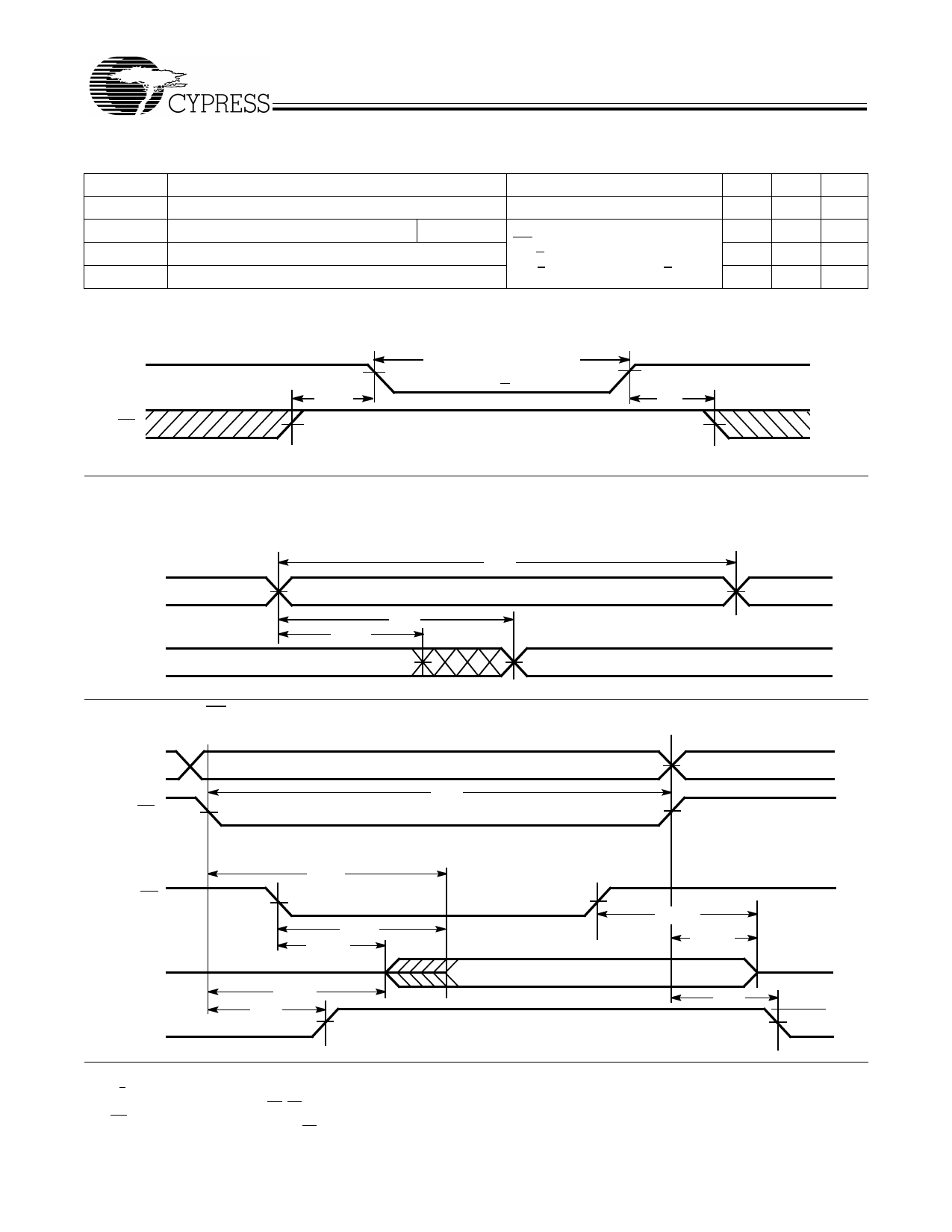
Data Retention Characteristics Over the Operating Range
Parameter
Description
Conditions[10]
VDR
ICCDR
tCDR[3]
tR[9]
VCC for Data Retention
Data Retention Current
Chip Deselect to Data Retention Time
Operation Recovery Time
Com’l
VCC = VDR = 2.0V,
CE > VCC – 0.3V
VIN > VCC – 0.3V or VIN < 0.3V
Data Retention Waveform
Min. Max Unit
2.0
V
200 µA
0
ns
10
µs
DATA RETENTION MODE
VCC
3.0V
VDR > 2V
tCDR
CE
Switching Waveforms
Read Cycle No. 1[11, 12]
tRC
ADDRESS
DATA OUT
tAA
tOHA
PREVIOUS DATA VALID
Read Cycle No. 2 (OE Controlled)[12, 13]
3.0V
tR
1046BV33–5
DATA VALID
1046BV33–6
ADDRESS
tRC
CE
tACE
OE
DATA OUT
VCC
SUPPLY
CURRENT
tDOE
tLZOE
HIGH IMPEDANCE
tLZCE
tPU
50%
Notes:
9. tr < 3 ns for the -10, -12, and -15 speeds.
10. No input may exceed VCC + 0.5V.
11. Device is continuously selected. OE, CE = VIL.
12. WE is HIGH for read cycle.
13. Address valid prior to or coincident with CE transition LOW.
Document #: 38-05170 Rev. **
DATA VALID
tHZOE
tHZCE
HIGH
IMPEDANCE
tPD
50%
ICC
ISB
1046BV33-7
Page 4 of 8
Share Link: 