VN1206L-GP013 Ver la hoja de datos (PDF) - Supertex Inc
Número de pieza
componentes Descripción
Fabricante
VN1206L-GP013 Datasheet PDF : 3 Pages
| |||
Supertex inc.
VN1206
N-Channel Enhancement-Mode
Vertical DMOS FET
Features
►► Free from secondary breakdown
►► Low power drive requirement
►► Ease of paralleling
►► Low CISS and fast switching speeds
►► Excellent thermal stability
►► Integral source-drain diode
►► High input impedance and high gain
Applications
►► Motor controls
►► Converters
►► Amplifiers
►► Switches
►► Power supply circuits
►► Drivers (relays, hammers, solenoids, lamps, memories,
displays, bipolar transistors, etc.)
General Description
This enhancement-mode (normally-off) transistor utilizes
a vertical DMOS structure and Supertex’s well-proven,
silicon-gate manufacturing process. This combination
produces a device with the power handling capabilities
of bipolar transistors and the high input impedance and
positive temperature coefficient inherent in MOS devices.
Characteristic of all MOS structures, this device is free
from thermal runaway and thermally-induced secondary
breakdown.
Supertex’s vertical DMOS FETs are ideally suited to a
wide range of switching and amplifying applications where
very low threshold voltage, high breakdown voltage, high
input impedance, low input capacitance, and fast switching
speeds are desired.
Ordering Information
Product Summary
Part Number
VN1206L-G
Package Option
TO-92
Packing
1000/Bag
BVDSS/BVDGS
RDS(ON)
(max)
IDSS
(min)
VN1206L-G P002
120V
6.0Ω
1.0A
VN1206L-G P003
VN1206L-G P005
TO-92
2000/Reel
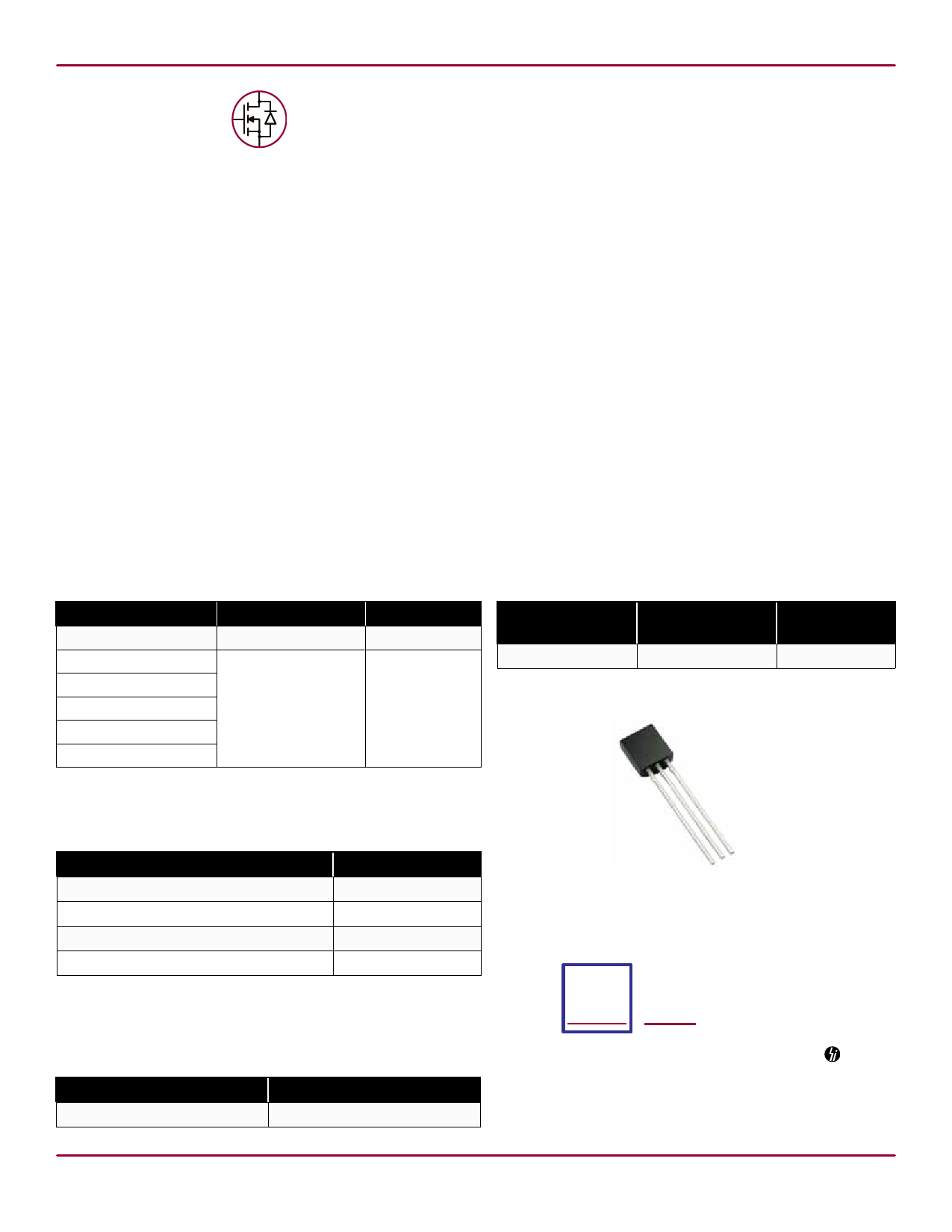
Pin Configuration
VN1206L-G P013
VN1206L-G P014
-G denotes a lead (Pb)-free / RoHS compliant package.
Contact factory for Wafer / Die availablity.
Devices in Wafer / Die form are lead (Pb)-free / RoHS compliant.
Absolute Maximum Ratings
SOURCE
DRAIN
Parameter
Value
Drain-to-source voltage
Drain-to-gate voltage
Gate-to-source voltage
BVDSS
BVDGS
±30V
Operating and storage temperature
-55OC to +150OC
Absolute Maximum Ratings are those values beyond which damage to the device may
occur. Functional operation under these conditions is not implied. Continuous operation
of the device at the absolute rating level may affect device reliability. All voltages are
referenced to device ground.
GATE
TO-92
Product Marking
Si VN YY = Year Sealed
1 2 0 6 L WW = Week Sealed
YYWW
= “Green” Packaging
Typical Thermal Resistance
Package
TO-92
θja
132OC/W
Package may or may not include the following marks: Si or
TO-92
Doc.# DSFP-VN1206
B081913
Supertex inc.
www.supertex.com
Share Link: 