ISL24010 Ver la hoja de datos (PDF) - Renesas Electronics
Número de pieza
componentes Descripción
Fabricante
ISL24010
Renesas Electronics

ISL24010 Datasheet PDF : 9 Pages
| |||
ISL24010
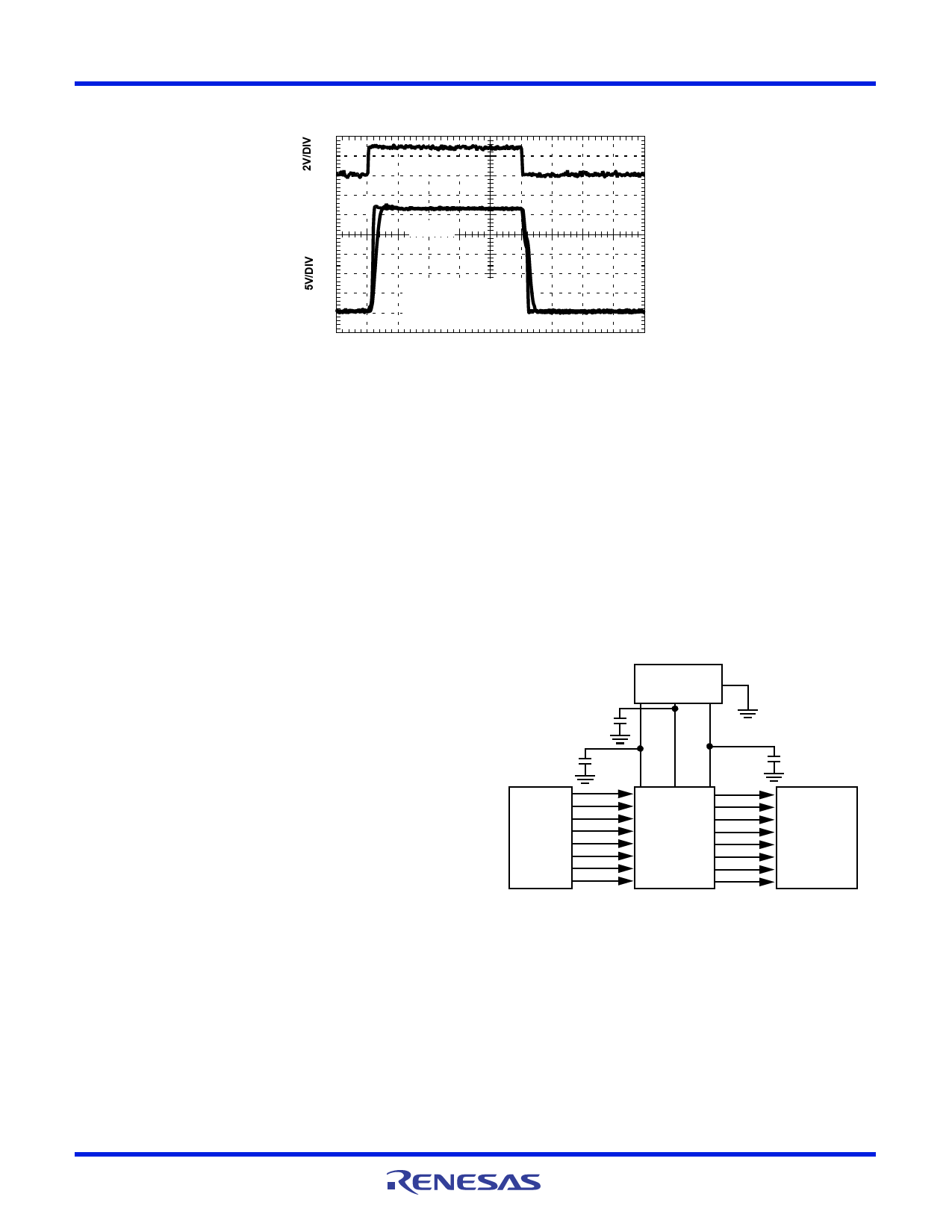
Typical Performance Curves TA = 25°C, Output load parallel RC (RL = 5k, CL = 100pF) unless otherwise specified. (Continued)
0
100pF
Pulse Input
1500pF
0
VON1 & 2 = 22V
VOFF = -5V
50kHz 50% Duty Cycle
2µs/DIV
FIGURE 13. TRANSIENT RESPONSE vs LOAD CAPACITANCE
Application Information
General
The ISL24010 is an Octal voltage level shifter. The part was
designed to level shifts a digital input signal to +22V and -5V
for TFT-LCD displays. The device is capable of level shifting a
CMOS logic signal between +40V and -20V.
Power Supply Decoupling
The ISL24010 requires a 0.1F decoupling capacitor as close
to the VON1, VON2 and VOFF power supply pins for a large
load equal to 5k in parallel with 100pF (Figure 16). This will
deduce any dv/dt between the different supplies and prevent
the internal ESD clamp from turning on and damaging the part.
Power Supply Sequence
The ISL24010 requires that VON2 be greater than or equal to
VON1 at all times. Therefore, if VON1 and Von 2 are different
supplies, then VON2 needs to be turned on before VON1. The
reason for this requirement is shown in Circuit 4 in the Pin
Description Table. The ESD protection diode between VON2
and Von 1 will forward bias if VON1 becomes a diode drop
greater than VON2. Recommended power supply sequence:
VON2, VON1, VOFF then input logic signals.
The ESD protection scheme is based on diodes from the pins
to the VON2 supply and a dV/dt- triggered clamp. This dV/dt
triggered clamp imposes a maximum supply turn-on slew rate
of 10V/µs. This clamp will trigger if the supply powers up too
fast, causing amps of current to flow. Ground and VON1 are
treated as I/O pins with this protection scheme. In applications
where the dV/dt supply ramp could exceed 10V/µs, such as hot
plugging, additional methods should be employed to ensure
the rate of rise is not exceeded.
Latch-up Proof
The ISL24010 is manufactured in a high voltage DI process
that isolates every transistor in it’s own tub making the part
latch-up proof.
Input Pin Connections
Unused inputs must be tied to ground. Failure to tie unused
input pins to ground will result in a rail to rail oscillations on the
respective output pins and higher unwanted power dissipation
in the part. Under these conditions, the temperature of the part
could get very hot.
Limiting the Output Current
No output short circuit current limit exists on this part. All
applications need to limit the output current to less than 80mA.
Adequate thermal heat sinking of the parts is also required.
Application Diagram (TV)
1.0F
1.0F
DC/DC
CONVERTER
VON1
VOFF
VON2
1.0F
TIMING
CON-
TROLLER
ISL24010
LEVEL
SHIFTER
LCD PANEL
FIGURE 14. TYPICAL TV APPLICATION CIRCUIT
FN6124 Rev 0.00
November 4, 2005
Page 7 of 9
Share Link: