EL7536 Ver la hoja de datos (PDF) - Renesas Electronics
Número de pieza
componentes Descripción
Fabricante
EL7536 Datasheet PDF : 9 Pages
| |||
EL7536
Absolute Maximum Ratings (TA = 25°C)
VIN, VDD, POR to SGND . . . . . . . . . . . . . . . . . . . . . . -0.3V to +6.5V
LX to PGND . . . . . . . . . . . . . . . . . . . . . . . . . . -0.3V to (VIN + +0.3V)
RSI, EN, VO, FB to SGND . . . . . . . . . . . . . . . -0.3V to (VIN + +0.3V)
PGND to SGND . . . . . . . . . . . . . . . . . . . . . . . . . . . . . -0.3V to +0.3V
Peak Output Current . . . . . . . . . . . . . . . . . . . . . . . . . . . . . . . . . 1.2A
Operating Ambient Temperature . . . . . . . . . . . . . . . .-40°C to +85°C
Storage Temperature . . . . . . . . . . . . . . . . . . . . . . . .-65°C to +150°C
Junction Temperature . . . . . . . . . . . . . . . . . . . . . . . . . . . . . . +125°C
CAUTION: Stresses above those listed in “Absolute Maximum Ratings” may cause permanent damage to the device. This is a stress only rating and operation of the
device at these or any other conditions above those indicated in the operational sections of this specification is not implied.
IMPORTANT NOTE: All parameters having Min/Max specifications are guaranteed. Typ values are for information purposes only. Unless otherwise noted, all tests are
at the specified temperature and are pulsed tests, therefore: TJ = TC = TA
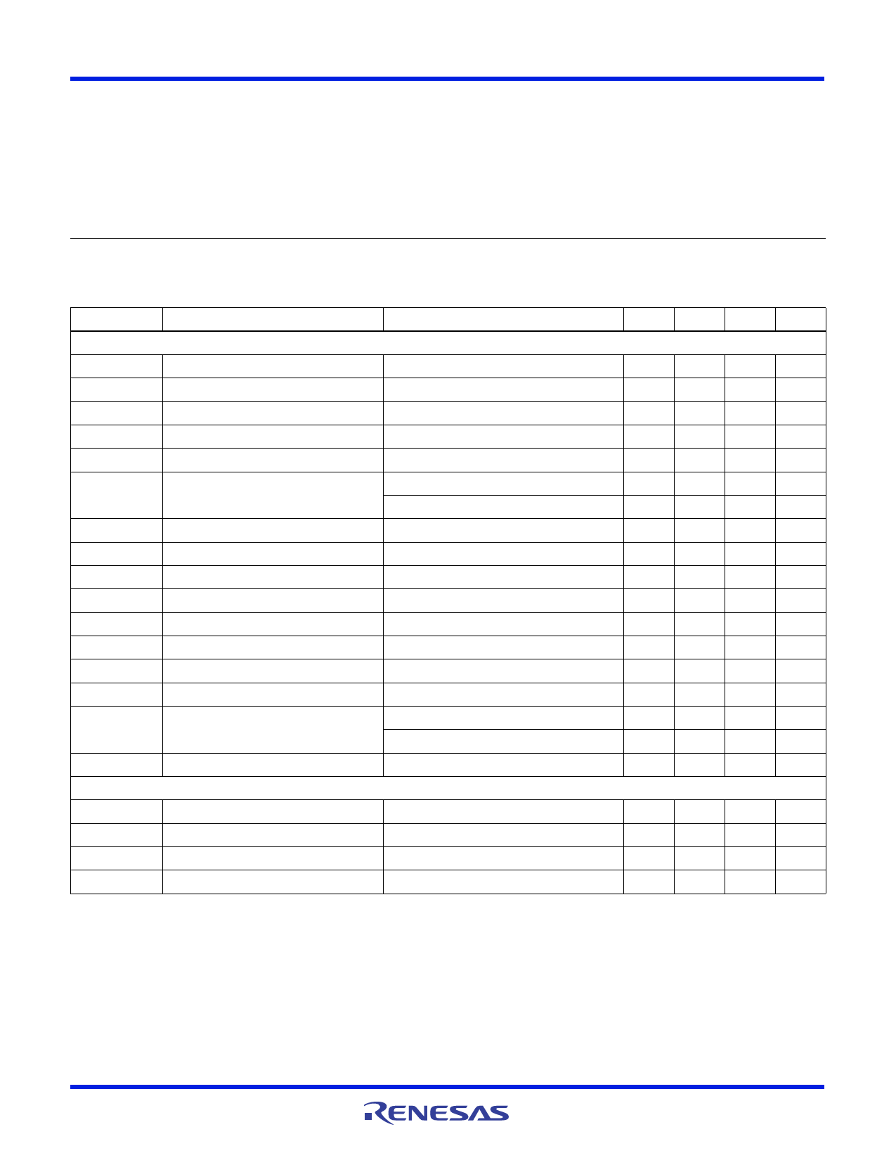
Electrical Specifications VDD = VIN = VEN = 3.3V, C1 = C2 = 10µF, L = 1.8µH, VO = 1.8V, unless otherwise specified.
PARAMETER
DESCRIPTION
CONDITIONS
MIN TYP MAX UNIT
DC CHARACTERISTICS
VFB
IFB
VIN, VDD
VIN,OFF
VIN,ON
IDD
Feedback Input Voltage
Feedback Input Current
Input Voltage
Minimum Voltage for Shutdown
Maximum Voltage for Startup
Supply Current
RDS(ON)-PMOS PMOS FET Resistance
RDS(ON)-NMOS NMOS FET Resistance
ILMAX
Current Limit
TOT,OFF
Over-temperature Threshold
TOT,ON
Over-temperature Hysteresis
IEN, IRSI
EN, RSI Current
VEN1, VRSI1 EN, RSI Rising Threshold
VEN2, VRSI2 EN, RSI Falling Threshold
VPOR
Minimum VFB for POR, WRT Targeted
VFB Value
VOLPOR
POR Voltage Drop
AC CHARACTERISTICS
VIN falling
VIN rising
PWM, VIN = VDD = 5V
EN = 0, VIN = VDD = 5V
VDD = 5V, wafer test only
VDD = 5V, wafer test only
T rising
T falling
VEN, VRSI = 0V and 3.3V
VDD = 3.3V
VDD = 3.3V
VFB rising
VFB falling
ISINK = 5mA
790
800
810
mV
250
nA
2.5
5.5
V
2
2.2
V
2.2
2.4
V
400
500
µA
0.1
1
µA
70
100
m
45
75
m
1.5
A
145
°C
130
°C
-1
1
V
2.4
V
0.8
V
95
%
86
%
35
70
mV
FPWM
tRSI
tSS
tPOR
PWM Switching Frequency
Minimum RSI Pulse Width
Soft-start Time
Power On Reset Delay Time
Guaranteed by design
1.4
1.5
1.75 MHz
25
50
ns
650
µs
80
100
120
ms
FN7396 Rev 8.00
July 13, 2006
Page 2 of 9
Share Link: 