ML9042 Ver la hoja de datos (PDF) - LAPIS Semiconductor Co., Ltd.
Número de pieza
componentes Descripción
Fabricante
ML9042 Datasheet PDF : 58 Pages
| |||
LAPIS Semiconductor
FEDL9042-01
ML9042-xx
I/O Characteristics
Parallel Interface Mode
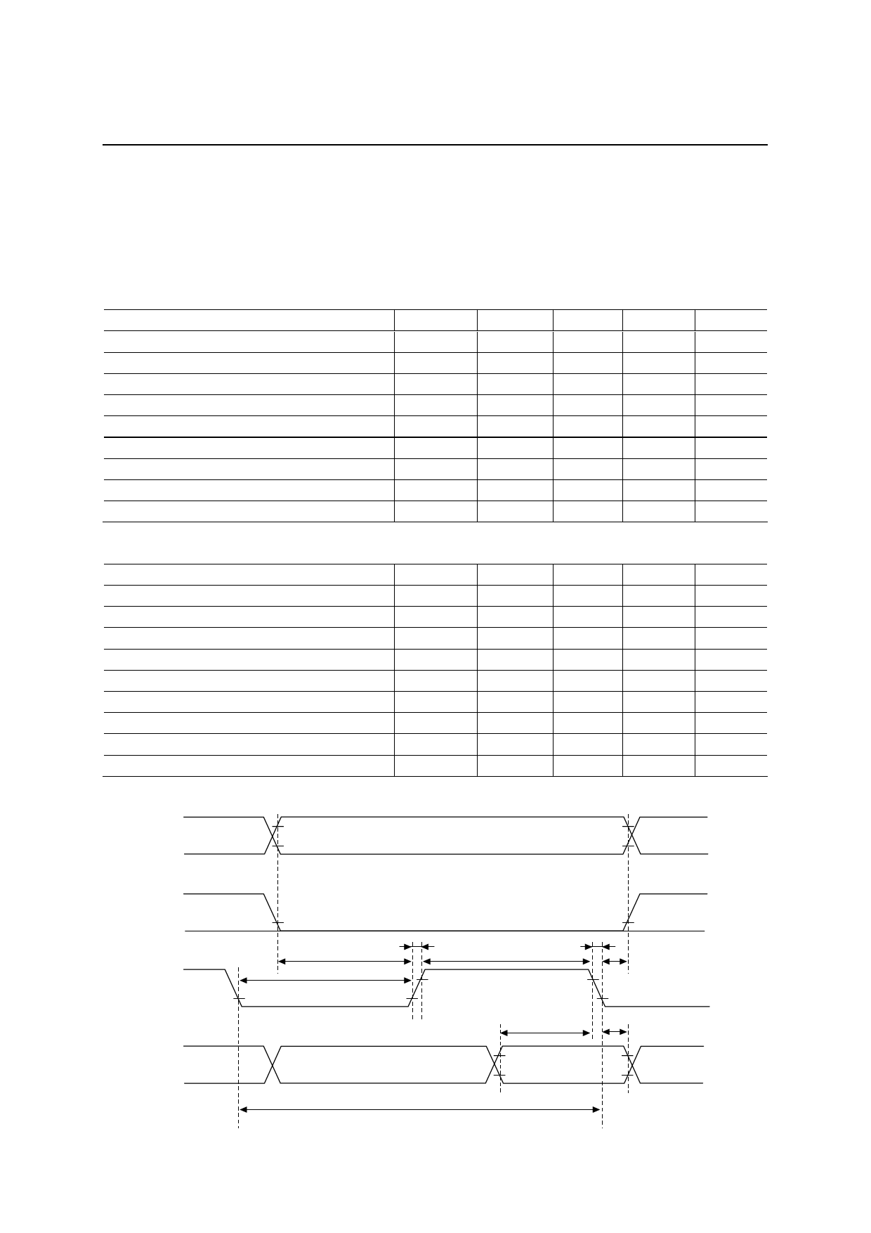
The timing for the input from the CPU and the timing for the output to the CPU are as shown below:
1) WRITE MODE (Timing for input from the CPU)
Parameter
RW/SI, RS0/CSB, RS1 Setup Time
E/SHTB Pulse Width
RW/SI, RS0/CSB, RS1 Hold Time
E/SHTB Rise Time
E/SHTB Fall Time
E/SHTB Pulse Width
E/SHTB Cycle Time
DB0(SO) to DB7 Input Data Setup Time
DB0(SO) to DB7 Input Data Hold Time
Symbol
tB
tW
tA
tr
tf
tL
tC
tI
tH
(VDD = 2.7 to 4.5 V, Ta = –40 to +85C)
Min.
Typ.
Max.
Unit
40
—
—
ns
450
—
—
ns
10
—
—
ns
—
—
125
ns
—
—
125
ns
430
—
—
ns
1000
—
—
ns
195
—
—
ns
10
—
—
ns
Parameter
RW/SI, RS0/CSB, RS1 Setup Time
E/SHTB Pulse Width
RW/SI, RS0/CSB, RS1 Hold Time
E/SHTB Rise Time
E/SHTB Fall Time
E/SHTB Pulse Width
E/SHTB Cycle Time
DB0(SO) to DB7 Input Data Setup Time
DB0(SO) to DB7 Input Data Hold Time
Symbol
tB
tW
tA
tr
tf
tL
tC
tI
tH
(VDD = 4.5 to 5.5 V, Ta = –40 to +85C)
Min.
Typ.
Max.
Unit
40
—
—
ns
220
—
—
ns
10
—
—
ns
—
—
125
ns
—
—
125
ns
220
—
—
ns
500
—
—
ns
60
—
—
ns
10
—
—
ns
RS1, RS0/CSB
VIH
VIL
VIH
VIL
RW/SI
E/SHTB
VIL
tB
tr
tL
VIH
VIL
VIL
DB0(SO) to DB7
tC
tW
tf
VIH
tI
VIL
tA
VIL
tH
VIH
Input
VIH
VIL
Data
VIL
11/58
Share Link: 