HV440WG-G Ver la hoja de datos (PDF) - Supertex Inc
Número de pieza
componentes Descripción
Fabricante
HV440WG-G Datasheet PDF : 6 Pages
| |||
HV440
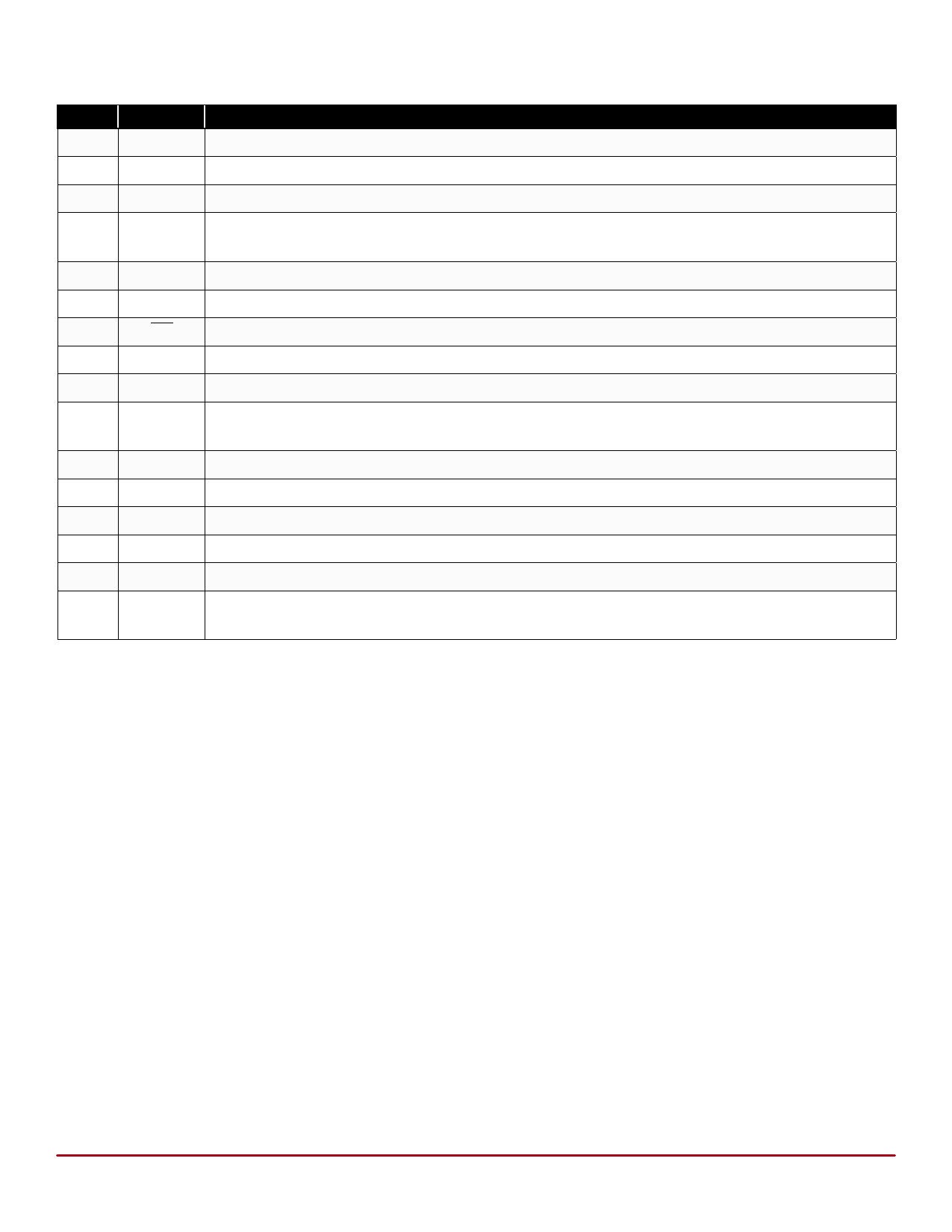
Pin Description
Pin
Name Description
1
VPP1 Positive high voltage supply.
2
PGND High voltage power ground.
3
GND Low voltage ground.
4
MODE
Logic mode input. Logic low activates 200nsec deadband. When mode is low, NIN turns on and off
the high voltage N- and P-Channels. Pin is not used and should be connected to VDD or ground.
5
PIN Logic control input. When mode is high, logic input high turns off output high voltage P-Channel.
6
NIN Logic control input. When mode is high, logic input high turns on output high voltage N-Channel.
7
EN Active low enable input.
8
VDD Logic supply voltage.
9
VNN1 Negative high voltage supply.
10
VNN2
Negative gate voltage supply. Generated by an internal linear regulator. A 0.1µF capacitor should
be connected between VNN2 and VNN1.
11
NGATE Gate drive for external N-channel MOSFET.
12 VNSEN Pulse by pulse over current sensing for internal N-Channel MOSFET.
13 HVOUT High voltage output. Voltage swings from VPP1 to VNN1.
14 VPSEN Pulse by pulse over current sensing for internal P-Channel MOSFET.
15
PGATE Gate drive for external P-channel MOSFET.
16
VPP2
Positive gate voltage supply. Generated by an internal linear regulator. A 0.1µF capacitor should
be connected between VPP2 and VPP1.
Doc.# DSFP - HV440
C031414
Supertex inc.
5
www.supertex.com
Share Link: 