HV582 Ver la hoja de datos (PDF) - Microchip Technology
Número de pieza
componentes Descripción
Fabricante
HV582 Datasheet PDF : 20 Pages
| |||
HV582
1.0 ELECTRICAL
CHARACTERISTICS
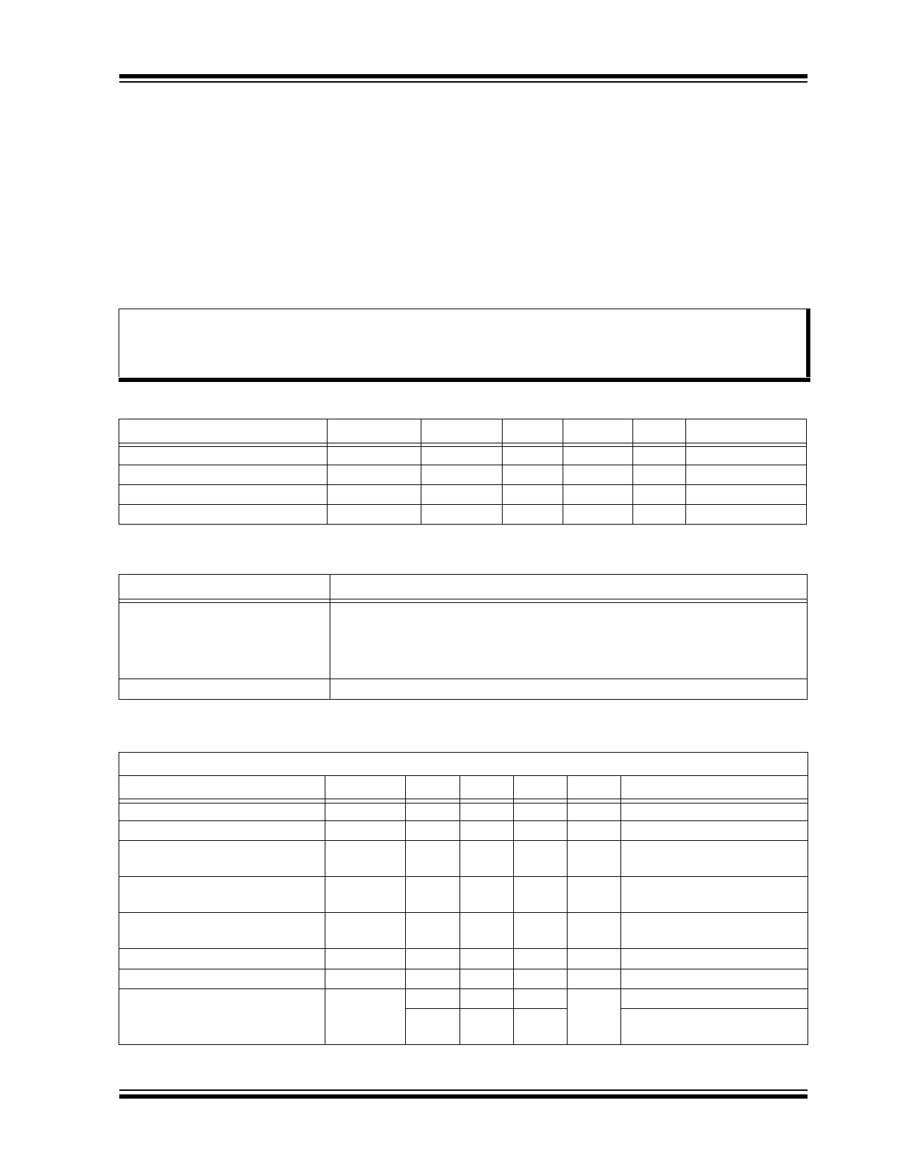
Absolute Maximum Rating†
Supply Voltage VDD.................................................................................................................................... -0.5V to +6.0V
High-Voltage Supply VPP .............................................................................................................................. VDD to +85V
Logic Input Voltages...........................................................................................................................-0.5V to VDD + 0.5V
Operating Junction Temperature.............................................................................................................-40°C to +125°C
Storage Temperature ..............................................................................................................................-65°C to +150°C
†Notice: Stresses above those listed under “Absolute Maximum Ratings” may cause permanent damage to the
device. This is a stress rating only and functional operation of the device at those or any other conditions, above those
indicated in the operational listings of this specification, is not implied. Exposure to maximum rating conditions for
extended periods may affect device reliability. Device is ESD sensitive. Use appropriate ESD precaution.
RECOMMENDED OPERATING CONDITIONS
Parameter
Symbol
Min.
Typ.
Logic Supply Voltage
High-Voltage Supply
High-Level Input Voltage
Low-Level Input Voltage
VDD
4.5
5.0
VPP
10
—
VIH
VDD – 0.9
—
VIL
0
—
Max.
5.5
80
VDD
0.9
Units
V
V
V
V
Conditions
TABLE 1-1: POWER SEQUENCES
Sequence Type
Steps
Power-Up Sequence
Power-Down Sequence
1. Connect Ground.
2. Apply VDD.
3. Set All Inputs (Data, CLK, etc.) to a known state.
4. Apply VPP.
Repeat the Power-Up sequence in reverse order.
DC ELECTRICAL CHARACTERISTICS
Electrical Specification: Unless otherwise specified, TA = TJ = +25°C, VDD = 5.0V and VPP = 80V.
Parameter
Symbol Min. Typ. Max. Units
Conditions
VPP Quiescent Supply Current
VDD Quiescent Supply Current
VDD Supply Current
IPPQ
IDDQ
IDD
–
–
100
µA
–
–
100
µA
–
–
25
mA fCLK= 30 MHz,
LE = low
High-Level Output Voltage
Output P-Channel Body Diode
Low-Level Output Voltage
Output N-Channel Body Diode
Logic Input High Current
HVOH
70
75
–
V IOUT = 75 mA,
VPP = 80V
HVOHD
–
–
83
V IOUT = -75 mA,
VPP = 80V (Note 1)
HVOL
–
5.0
10
V IOUT = -75 mA
HVOLD
-3.0
–
–
V IOUT = 75 mA (Note 1)
IIH
–
–
1.0
µA VIH = VDD
10
30
50
VIH = VDD,
RST and POL only
Note 1: Specification is for design guidance only.
2015 Microchip Technology Inc.
DS20005455A-page 3
Share Link: 