CMX635 Ver la hoja de datos (PDF) - MX-COM Inc
Número de pieza
componentes Descripción
Fabricante
CMX635 Datasheet PDF : 88 Pages
| |||
ISDN subscriber Processor
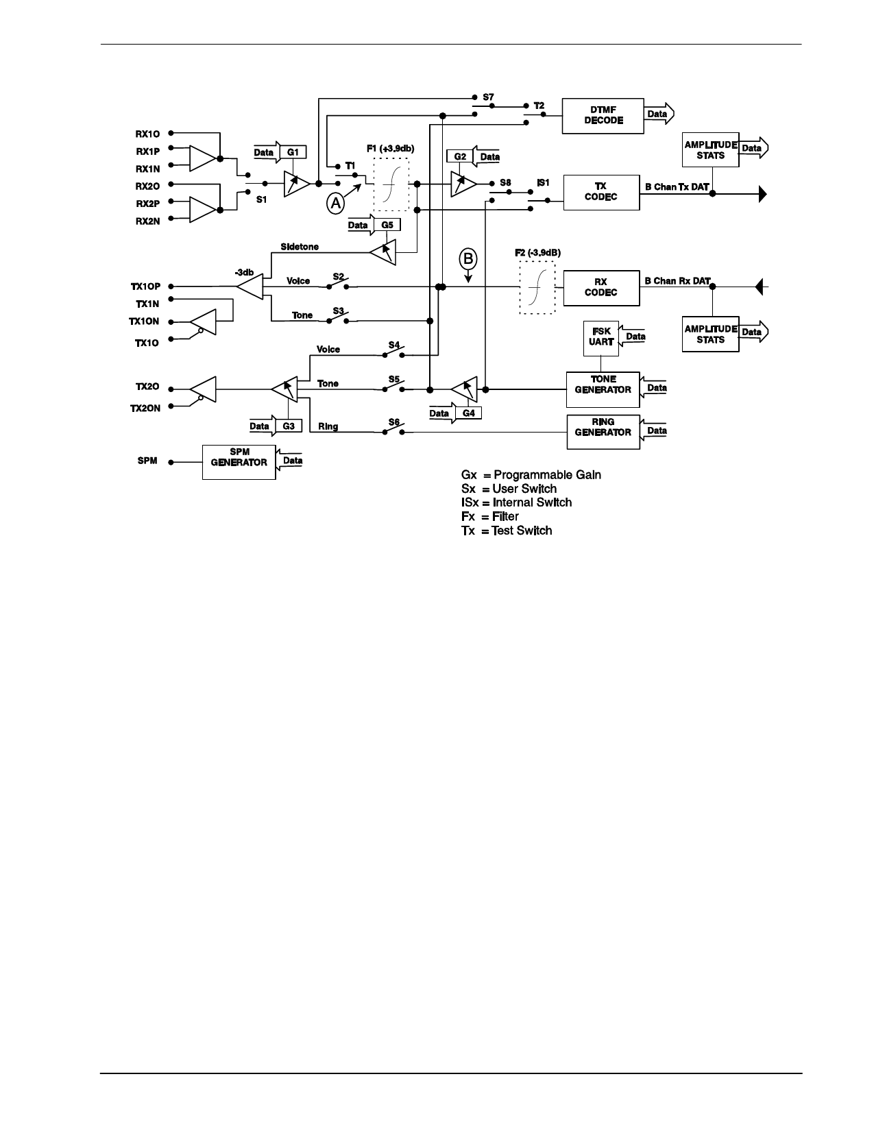
1.2 Analog Block Diagram
Page 6 of 88
CMX635 Advance Information
Notes:
G1 =
G2 =
G3 =
G4 =
G5 =
Figure 2: Analog Block Diagram
0dB to 22.5dB ( in 1.5db steps) -
Level set/AGC gain.
0dB to –42dB (in 3dB steps + mute) - Speakerphone attenuation.
+6dB to –42dB (in 0.5dB steps + mute) - Speaker/ring output gain.
0dB to –42dB (in 3dB steps + mute) - Tone gain
-6dB to –36dB (in 2dB steps) -
Sidetone gain.
S1 – S8
=
User selectable switches.
IS1
=
Internally operated switches (shown for information only).
T1 - T2
=
Test Switches (shown for information only).
At reference points “A” and “B” the nominal signal level scaling as defined in ITU-T G714 is:
0dbm0 ≡ 0dBm = 775 mV r.m.s. at 5V power supply.
The maximum unclipped sine wave possible on reference points “A” and “B” is:
3.14dbm0 ≡ 3.14dBm = 1.11 V r.m.s. for A law companding at 5 V supply.
Peak to peak full scale input signal to Rx Codec is 0.986 x VDD for A-law companding,
And 0.989 x VDD for µ-law companding.
2001 MX-COM, Inc.
www.mxcom.com Tel: 800 638 5577 336 744 5050 Fax: 336 744 5054
Doc. # 20480225.002
4800 Bethania Station Road, Winston-Salem, NC 27105-1201 USA All trademarks and service marks are held by their respective companies.
Share Link: 