LC75813E Ver la hoja de datos (PDF) - ON Semiconductor
Número de pieza
componentes Descripción
Fabricante
LC75813E Datasheet PDF : 28 Pages
| |||
LC75813E, LC75813T
Specifications
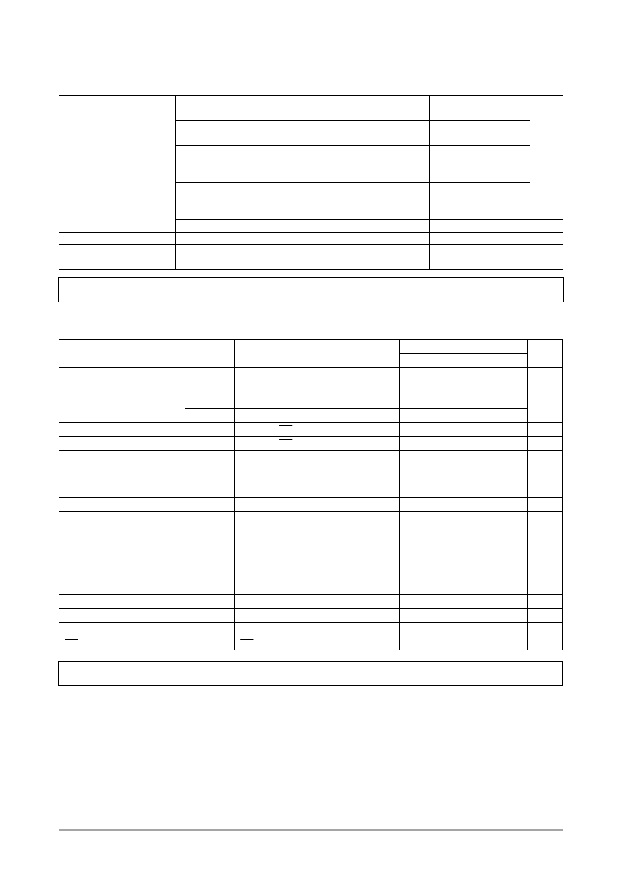
Absolute Maximum Ratings at Ta = 25C, VSS = 0 V
Parameter
Symbol
Conditions
Maximum supply voltage
Input voltage
Output voltage
Output current
Allowable power dissipation
VDD max
VLCD max
VIN1
VIN2
VIN3
VOUT1
VOUT2
IOUT1
IOUT2
IOUT3
Pd max
VDD
VLCD
CE, CL, DI, INH
OSC
VLCD1, VLCD2
OSC
S1 to S87, COM1 to COM4, P1 to P8
S1 to S87
COM1 to COM4
P1 to P8
Ta = 85°C
Operating temperature
Topr
Storage temperature
Tstg
Ratings
unit
–0.3 to +7.0
–0.3 to +7.0
V
–0.3 to +7.0
–0.3 to VDD +0.3
V
–0.3 to VLCD +0.3
–0.3 to VDD +0.3
V
–0.3 to VLCD +0.3
300
A
3 mA
5 mA
200 mW
–40 to +85
C
–55 to +125
C
Stresses exceeding those listed in the Maximum Ratings table may damage the device. If any of these limits are exceeded, device functionality should not be assumed,
damage may occur and reliability may be affected.
Allowable Operating Ranges at Ta = 40 to +85C, VSS = 0 V
Parameter
Supply voltage
Input voltage
Input high-level voltage
Input low-level voltage
Recommended external
resistance
Recommended external
capacitance
Guaranteed oscillation range
Data setup time
Data hold time
CE wait time
CE setup time
CE hold time
High-level clock pulse width
Low-level clock pulse width
Rise time
Fall time
INH switching time
Symbol
VDD
VLCD
VLCD1
VLCD2
VIH
VIL
ROSC
COSC
fOSC
tds
tdh
tcp
tcs
tch
tH
tL
tr
tf
tc
Conditions
VDD
VLCD
VLCD1
VLCD2
CE, CL, DI, INH
CE, CL, DI, INH
OSC
OSC
OSC
CL, DI : Figure 2
CL, DI : Figure 2
CE, CL : Figure 2
CE, CL : Figure 2
CE, CL : Figure 2
CL : Figure 2
CL : Figure 2
CE, CL, DI : Figure 2
CE, CL, DI : Figure 2
INH, CE : Figure 3
Ratings
Unit
min
typ
max
2.7
6.0
V
2.7
6.0
2/3VLCD
1/3VLCD
VLCD
V
VLCD
0.8VDD
6.0
V
0
0.2VDD
V
39
k
1000
19
38
160
160
160
160
160
160
160
160
160
10
pF
76 kHz
ns
ns
ns
ns
ns
ns
ns
ns
ns
s
Functional operation above the stresses listed in the Recommended Operating Ranges is not implied. Extended exposure to stresses beyond the Recommended
Operating Ranges limits may affect device reliability.
www.onsemi.com
2
Share Link: 