LC75813E(2013) Ver la hoja de datos (PDF) - ON Semiconductor
Número de pieza
componentes Descripción
Fabricante
LC75813E Datasheet PDF : 26 Pages
| |||
LC75813E, 75813T
Pin Functions
Symbol
S1/P1 to S8/P8
S9 to S86
Pin No.
LC75813E LC75813T
Function
3 to 10 1 to 8 Segment outputs for displaying the display data transferred by serial data
input. The pins S1/P1 to S8/P8 can be used as general-purpose output
11 to 88 9 to 86 ports when so set up by the control data.
COM1 to COM3
COM4/S87
92 to 90 90 to 88 Common driver outputs.
89
87 The frame frequency is fO Hz.
The COM4/S87 pin can be used as a segment output in 1/3 duty.
OSC
CE
CL
DI
INH
Oscillator connection.
98
96 An oscillator circuit is formed by connecting an external resistor and
capacitor to this pin.
100
98 Serial data transfer inputs. These pins are connected to the control
microprocessor.
1
99 CE: Chip enable
CL: Synchronization clock
2
100 DI: Transfer data
Display off control input
• INH = low (VSS) ....Off
S1/P1 to S8/P8 = low (VSS)
(These pins are forcibly set to the segment output port
99
97
function and fixed at the VSS level.)
S9 to S86 = low (VSS)
COM1 to COM3 = low (VSS)
COM4/S87 = low (VSS)
• INH = high (VDD) ..On
Note that serial data transfers can be performed when the display is forced
off by this pin.
VLCD1
Used to apply the LCD drive 2/3 bias voltage externally. This pin must be
95
93 connected to VLCD2 when 1/2 bias drive is used.
VLCD2
VDD
VLCD
VSS
Used to apply the LCD drive 1/3 bias voltage externally. This pin must be
96
94 connected to VLCD1 when 1/2 bias drive is used.
93
91 Logic block power supply. Provide a voltage in the range 2.7 to 6.0 V.
94
92 LCD driver block power supply. Provide a voltage in the range 2.7 to 6.0 V.
97
95 Ground pin. Connect to ground.
Active
Handling
I/O when unused
—
O
Open
—
O
Open
—
I/O
VDD
H
I
I
GND
—
I
L
I
GND
—
I
Open
—
I
Open
—
—
—
—
—
—
—
—
—
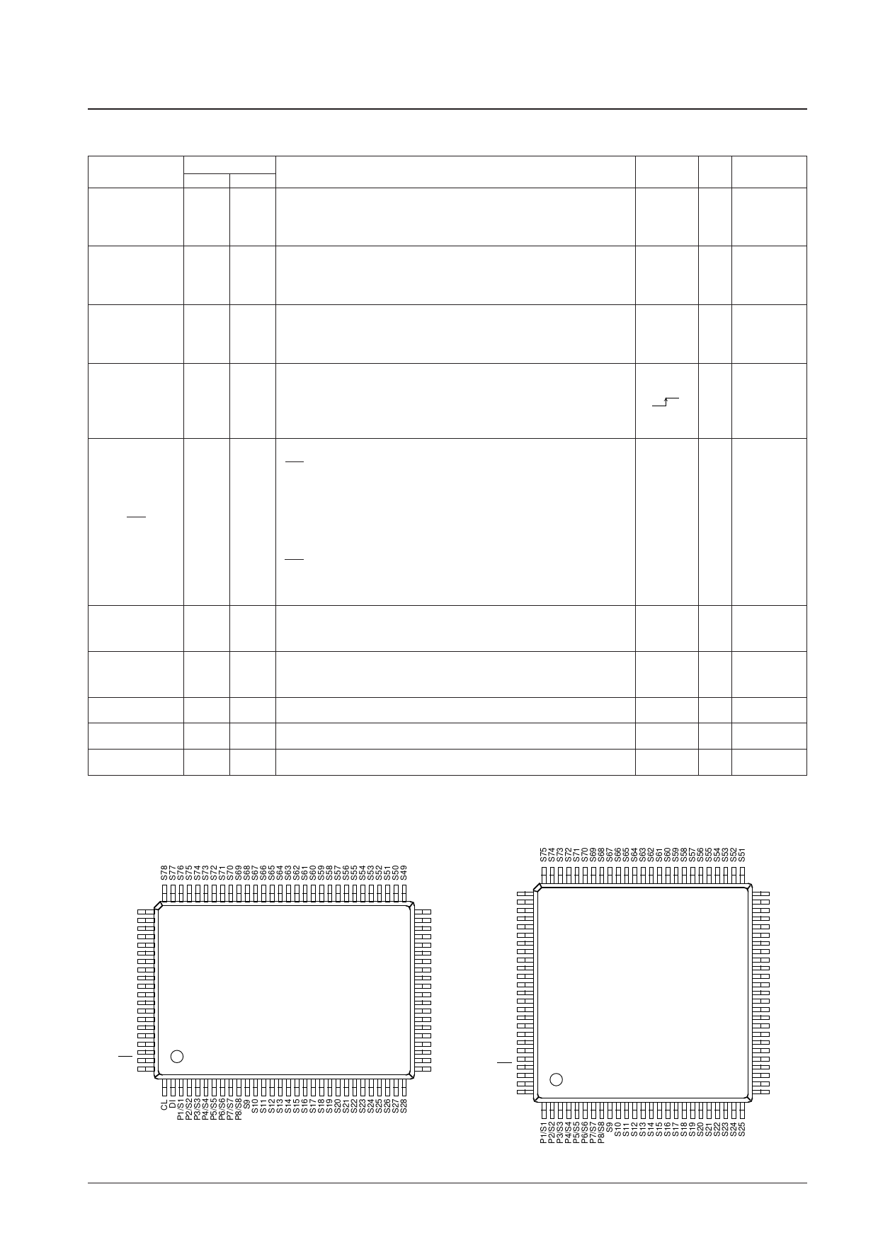
Pin Assignments
80
81
S79
S80
S81
S82
S83
S84
S85
S86
S87/COM4
COM3
COM2
COM1
VDD
VLCD
VLCD1
VLCD2
VSS
OSC
INH
CE
100
1
LC75813E
(QFP100E)
51
50
S48
S47
S46
S45
S44
S43
S42
S41
S40
S39
S38
S37
S36
S35
S34
S33
S32
S31
S30
S29
31
30
75
76
S76
S77
S78
S79
S80
S81
S82
S83
S84
S85
S86
S87/COM4
COM3
COM2
COM1
VDD
VLCD
VLCD1
VLCD2
VSS
OSC
INH
CE
CL
DI
100
1
LC75813T
(TQFP100)
51
50
S50
S49
S48
S47
S46
S45
S44
S43
S42
S41
S40
S39
S38
S37
S36
S35
S34
S33
S32
S31
S30
S29
S28
S27
S26
26
25
Top view
No. 7159-5/26
Share Link: 