CXA1700AQ Ver la hoja de datos (PDF) - Sony Semiconductor
Número de pieza
componentes Descripción
Fabricante
CXA1700AQ Datasheet PDF : 51 Pages
| |||
CXA1700AQ/AR
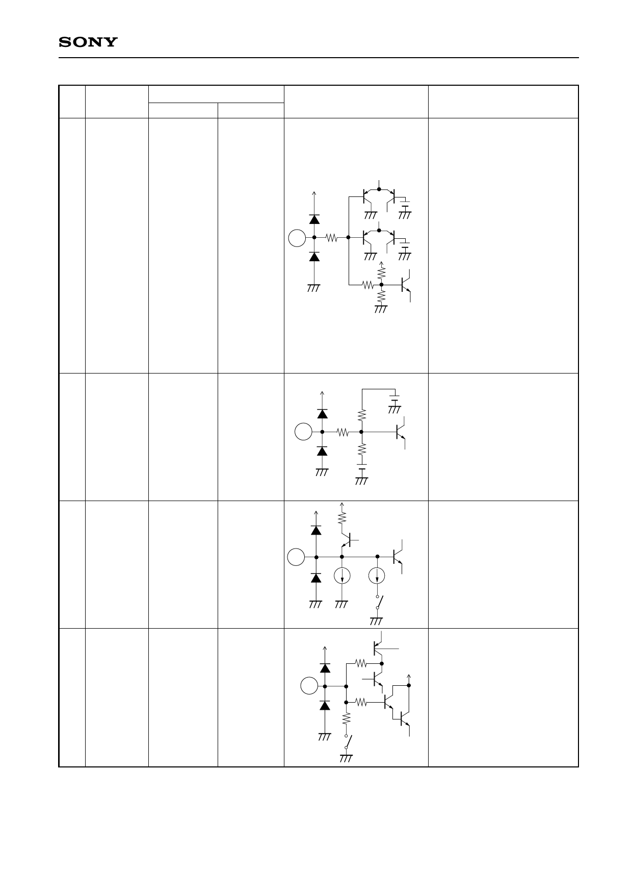
Pin
Symbol
No.
Pin voltage
DC
AC
26 DDS/MASK 2.0V
—
(when open)
(MASK)
1.5V
(DDS)
2.3 to 3.0V
Equivalent circuit
Description
Input for VOW (character
level) signal, VOB (character
background) timing pulse of
DDS (date display system)
2.0V and masking timing pulse.
MASK : VTH = 1.1V
150
26
DDS : VTH = 2.0V
1.1V
By varying the input DC for
DDS over a range of 2.3V to
45k 16k
15k
3.0V, the character level can
be changed.
(Refer to item 4 on Description
of Operation.)
27 WDC
2.6V
—
(when open)
28 V IN2
2.05V
(sync tip
level)
Video
500mVp-p
input
29 AGC TC1
—
—
27
28
29
4.1V
30k
150
10k
2.05V
270
100nA
4µA
MUTE
ON
Determines the white/dark
clipping levels. When open,
the standard white clipping
level is 235%, and the dark
clipping level is 95%.
(Mode DC1, 2 = Low, High)
(Refer to item 5 on Description
of Operation.)
Video signal input. Performs
diode clamping, with the
clamp capacitance externally
connected. If the mode MUTE
is set High, the charge of the
clamp capacitance is
discharged.
Time constant for the video
100
AGC circuit in the I/O block.
During mute and playback, the
charge of the external
1k
capacitance is discharged.
47k
MUTE ON
PB ON
—9—
Share Link: 