CXA1700AQ Ver la hoja de datos (PDF) - Sony Semiconductor
Número de pieza
componentes Descripción
Fabricante
CXA1700AQ Datasheet PDF : 51 Pages
| |||
CXA1700AQ/AR
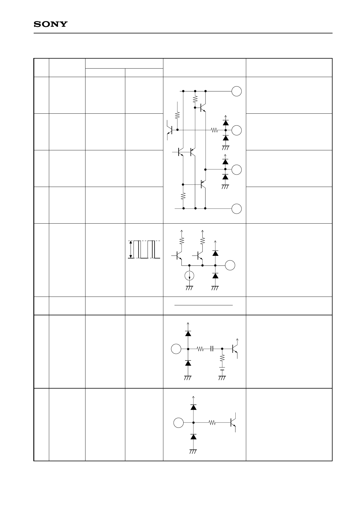
Pin
Symbol
No.
35 VOUT GND 0V
Pin voltage
DC
AC
—
Equivalent circuit
Description
GND for the video out circuit.
38
36 VIDEO
OUT
1.6V
(sync tip
level)
Video
2.0Vp-p
output
37 INV IN
1.5V
Video
1.0Vp-p
input
38 RF/V VCC VCC=4.75V
—
Video out 75Ω driver output.
100
37
Inverted input for V sag
compensation for the video
36
out 75Ω driver.
Video out circuit and RF
system block power supply.
35
39 Y RF OUT 2.1V
Y FM output
63
63
500mVp-p
2.5mA
During recording, FM-
modulated Y signal output.
If mode TEST2 is set High
during recording, the Y signal
39 after white/dark clipping is
output.
40 RF GND 0V
41 Y RF IN
—
—
YFM
200mVp-p
input
150 10p
41
45k
RF block GND.
During playback, inputs Y-RF
signal to FM modulation
circuit.
42 SMEAR Control
—
CONT
range:
1.8V to Vcc
150
42
During recording, adjustment
for high Luminance Smear
Compensation.
—11—
Share Link: 