SSF2301 Ver la hoja de datos (PDF) - GOOD-ARK
Número de pieza
componentes Descripción
Fabricante
SSF2301 Datasheet PDF : 7 Pages
| |||
SSF2301
20V P-Channel MOSFET
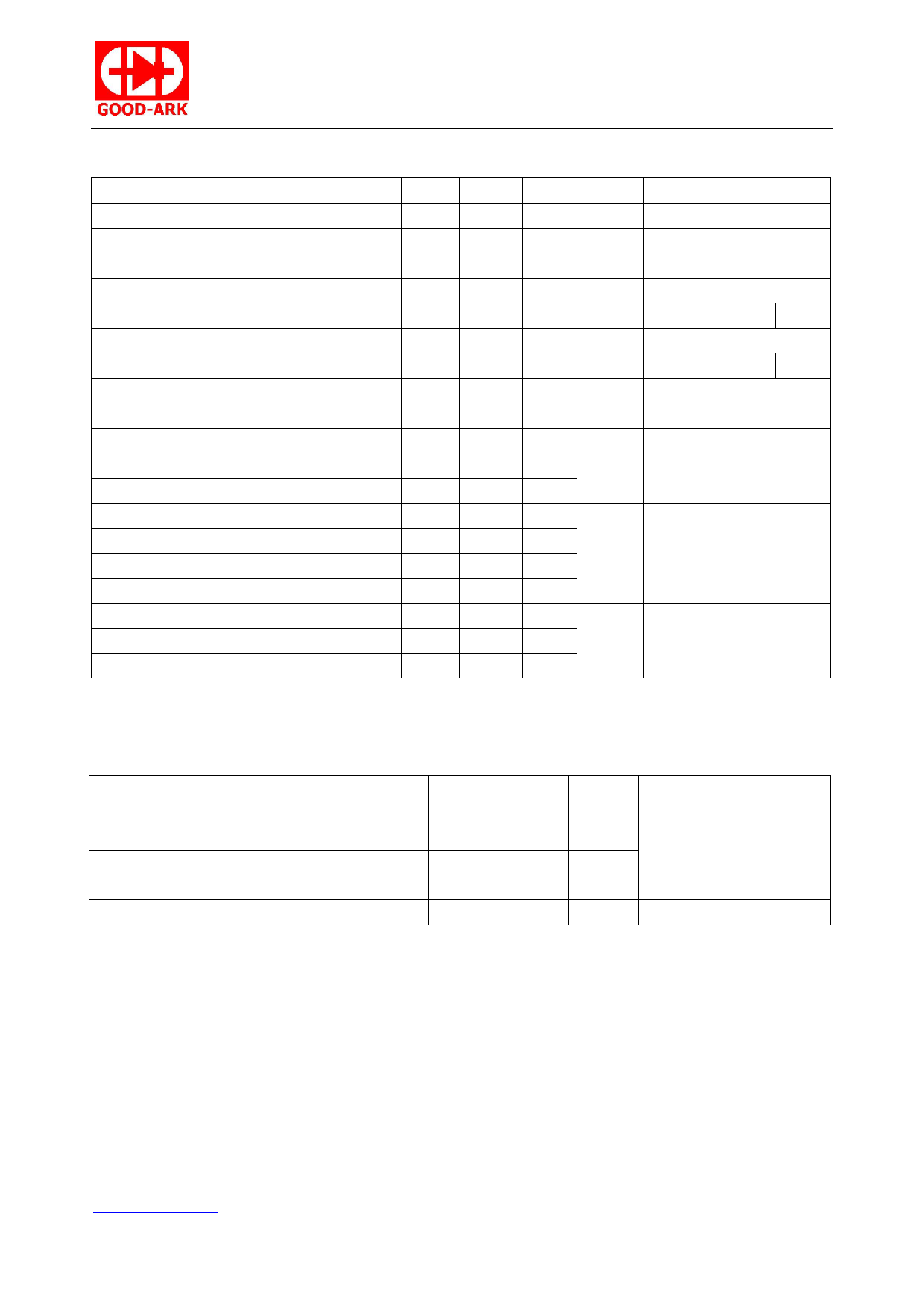
Electrical Characteristics @TA=25℃ unless otherwise specified
Symbol Parameter
V(BR)DSS Drain-to-Source breakdown voltage
RDS(on) Static Drain-to-Source on-resistance
VGS(th) Gate threshold voltage
IDSS
Drain-to-Source leakage current
IGSS
Gate-to-Source forward leakage
Qg
Total gate charge
Qgs
Gate-to-Source charge
Qgd
Gate-to-Drain("Miller") charge
td(on)
Turn-on delay time
tr
Rise time
td(off)
Turn-Off delay time
tf
Fall time
Ciss
Input capacitance
Coss
Output capacitance
Crss
Reverse transfer capacitance
Min.
-20
—
—
-0.5
—
—
—
—
—
—
—
—
—
—
—
—
—
—
—
Typ.
—
60
85
—
-0.58
—
—
—
—
9.6
1.1
2.6
9.7
18
25
31
490
75
60
Max.
—
90
115
-1
—
-1
-50
100
-100
—
—
—
—
—
—
—
—
—
—
Units
V
mΩ
V
μA
nA
nC
Conditions
VGS = 0V, ID = -250μA
VGS=-4.5V,ID = -3A
VGS=-2.5V,ID = -2A
VDS = VGS, ID = -250μA
TJ = 125°C
VDS = -20V,VGS = 0V
TJ = 125°C
VGS =12V
VGS = -12V
ID = -3A,
VDS=-10V,
VGS = -4.5V
VGS=-4.5V, VDS =-20V,
ns
RGEN=3Ω
VGS = 0V,
pF VDS =-10V,
ƒ = 1MHz
Source-Drain Ratings and Characteristics
Symbol
IS
ISM
VSD
Parameter
Continuous Source Current
(Body Diode)
Pulsed Source Current
(Body Diode)
Diode Forward Voltage
Min.
—
—
—
Typ.
—
—
-0.83
Max.
-3 ①
-10
-1.2
Units
A
A
V
Conditions
MOSFET symbol
showing the
integral reverse
p-n junction diode.
IS=-0.75A, VGS=0V
www.goodark.com
Page 2 of 7
Rev.2.1
Share Link: 