SI2328DS-T1-E3(2011) Ver la hoja de datos (PDF) - Vishay Semiconductors
Número de pieza
componentes Descripción
Fabricante
SI2328DS-T1-E3 Datasheet PDF : 8 Pages
| |||
Si2328DS
Vishay Siliconix
SPECIFICATIONS (TA = 25 °C, unless otherwise noted)
Parameter
Symbol
Test Conditions
Static
Drain-Source Breakdown Voltage
Gate-Threshold Voltage
Gate-Body Leakage
Zero Gate Voltage Drain Current
On-State Drain Currenta
Drain-Source On-Resistancea
Forward Transconductancea
Diode Forward Voltage
Dynamicb
VDS
VGS(th)
IGSS
IDSS
ID(on)
RDS(on)
gfs
VSD
VGS = 0 V, ID = 1 mA
VDS = VGS, ID = 250 µA
VDS = 0 V, VGS = ± 20 V
VDS = 100 V, VGS = 0 V
VDS = 100 V, VGS = 0 V, TJ = 70 °C
VDS 15 V, VGS = 10 V
VGS = 10 V, ID = 1.5 A
VDS = 15 V, ID = 1.5 A
IS = 1 A, VGS = 0 V
Total Gate Charge
Gate-Source Charge
Gate-Drain Charge
Gate Resistance
Switching
Qg
Qgs
VDS = 50 V, VGS = 10 V, ID = 1.5 A
Qgd
Rg
Turn-On Delay Time
td(on)
Rise Time
Turn-Off Delay Time
tr
td(off)
VDD = 50 V, RL = 33
ID 0.2 A, VGEN = 10 V, Rg = 6
Fall Time
tf
Source-Drain Reverse Recovery Time
trr
IF = 1.5 A, dI/dt = 100 A/µs
Notes:
a. Pulse test: PW 300 µs, duty cycle 2 %.
b. Guaranteed by design, not subject to production testing.
Limits
Min.
Typ.
Max.
Unit
100
V
2
4
± 100
nA
1
µA
75
6
A
0.195 0.250
4
S
0.8
1.2
V
3.3
5
0.47
nC
1.45
0.5
1.3
2.4
7
11
11
17
9
15
ns
10
15
50
100
Stresses beyond those listed under “Absolute Maximum Ratings” may cause permanent damage to the device. These are stress ratings only, and functional operation
of the device at these or any other conditions beyond those indicated in the operational sections of the specifications is not implied. Exposure to absolute maximum
rating conditions for extended periods may affect device reliability.
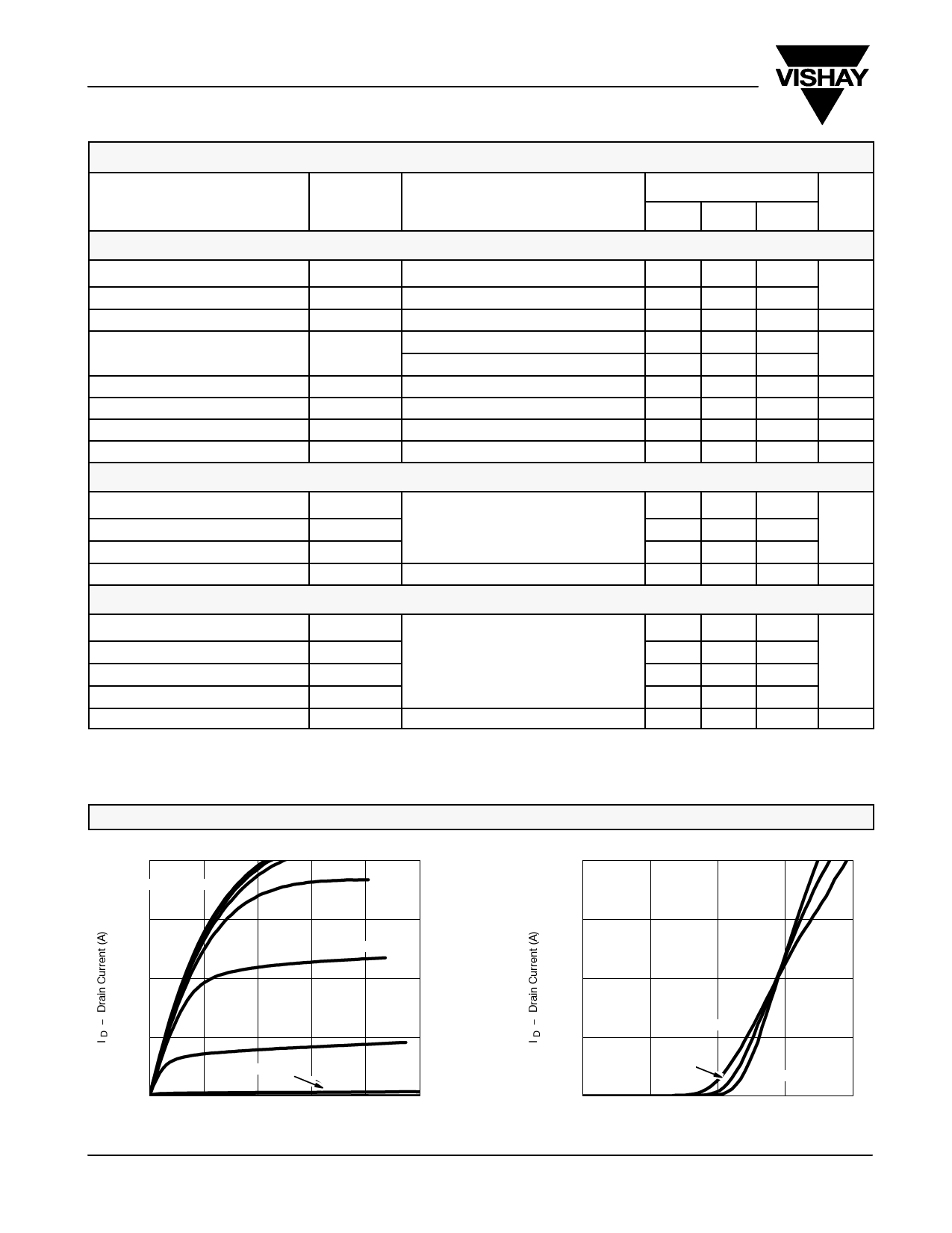
TYPICAL CHARACTERISTICS (25 °C, unless otherwise noted)
12
12
VGS = 10 V, 9 V, 8 V
7V
9
9
6V
6
6
5V
3
3 V, 2 V, 1 V
4V
0
0
2
4
6
8
10
VDS - Drain-to-Source Voltage (V)
Output Characteristics
TC = 125 °C
3
25 °C
- 55 °C
0
0
2
4
6
8
VGS - Gate-to-Source Voltage (V)
Transfer Characteristics
www.vishay.com
Document Number: 71796
2
S11-2000-Rev. F, 10-Oct-11
This document is subject to change without notice.
THE PRODUCTS DESCRIBED HEREIN AND THIS DOCUMENT ARE SUBJECT TO SPECIFIC DISCLAIMERS, SET FORTH AT www.vishay.com/doc?91000
Share Link: 