SPT9689 Ver la hoja de datos (PDF) - Cadeka Microcircuits LLC.
Número de pieza
componentes Descripción
Fabricante
SPT9689 Datasheet PDF : 8 Pages
| |||

TEST LEVEL CODES
All electrical characteristics are subject to the
following conditions:
All parameters having min/max specifications
are guaranteed. The Test Level column indi-
cates the specific device testing actually per-
formed during production and Quality Assur-
ance inspection. Any blank section in the data
column indicates that the specification is not
tested at the specified condition.
LEVEL
I
II
III
IV
V
VI
TEST PROCEDURE
100% production tested at the specified temperature.
100% production tested at TA = +25 °C, and sample tested at the
specified temperatures.
QA sample tested only at the specified temperatures.
Parameter is guaranteed (but not tested) by design and characteri-
zation data.
Parameter is a typical value for information purposes only.
100% production tested at TA = +25 °C. Parameter is guaranteed
over specified temperature range.
TIMING INFORMATION
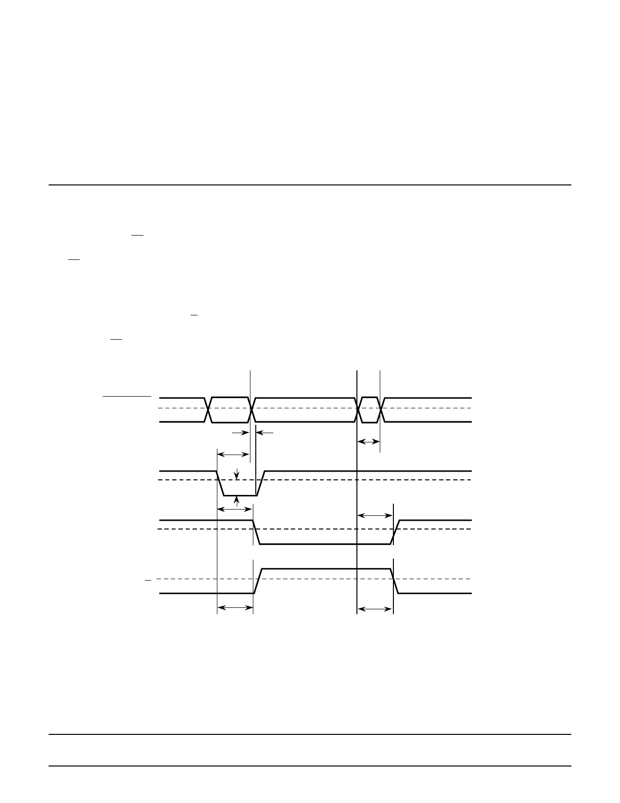
The timing diagram for the comparator is shown in figure
1. If LE is high and LE low in the SPT9689, the comparator
tracks the input difference voltage. When LE is driven low
and LE high, the comparator outputs are latched into their
existing logic states.
The leading edge of the input signal (which consists of a
20 mV overdrive voltage) changes the comparator output
after a time of tpdL or tpdH (Q or Q). The input signal must
be maintained for a time tS (set-up time) before the LE fall-
ing edge and LE rising edge and held for time tH after the
falling edge for the comparator to accept data. After tH, the
output ignores the input status until the latch is strobed
again. A minimum latch pulse width of tpL is needed for
strobe operation, and the output transitions occur after a
time of tpLOH or tpLOL.
The set-up and hold times are a measure of the time
required for an input signal to propagate through the first
stage of the comparator to reach the latching circuitry.
Input signals occurring before tS will be detected and held;
those occurring after tH will not be detected. Changes
between tS and tH may not be detected.
Figure 1 – Timing Diagram
Latch Enable
Latch Enable
Differential
Input Voltage
Output Q
tH
tS
VOD
tpdL
tpL
tpLOH
50%
VREF ± VOS
50%
Output Q
tpdH
tpLOL
VIN+=100 mV (p-p), VOD=20 mV
50%
SPT9689
3
2/20/01