MAX4514 Ver la hoja de datos (PDF) - Maxim Integrated
Número de pieza
componentes Descripción
Fabricante
MAX4514 Datasheet PDF : 8 Pages
| |||
Low-Voltage, Low-On-Resistance,
SPST, CMOS Analog Switches
ABSOLUTE MAXIMUM RATINGS
(Voltages referenced to GND.)
V+ ..............................................................................-0.3V, +13V
Voltage into Any Terminal (Note 1)...............-0.3V to (V+ + 0.3V)
or ±20mA (whichever occurs first)
Continuous Current into Any Terminal..............................±20mA
Peak Current, NO_ or COM_
(pulsed at 1ms,10% duty cycle)....................................±30mA
ESD per Method 3015.7 ..................................................>2000V
Continuous Power Dissipation (TA = +70°C)
8-Pin Plastic DIP (derate 9.09mW/°C above +70°C) ....727mW
8-Pin SO (derate 5.88mW/°C above +70°C).................471mW
5-Pin SOT23-5 (derate 7.1mW/°C above +70°C) .........571mW
8-Pin CERDIP (derate 8.00mW/°C above +70°C).........640mW
Operating Temperature Ranges
MAX4514C_ _/MAX4515C_ _ ..............................0°C to +70°C
MAX4514E_ _/MAX4515E_ _ ............................-40°C to +85°C
MAX4514MJA/MAX4515MJA .........................-55°C to +125°C
Storage Temperature Range .............................-65°C to +150°C
Lead Temperature (soldering, 10s) .................................+300°C
Note 1: Voltages exceeding V+ or GND on any signal terminal are clamped by internal diodes. Limit forward-diode current to
maximum current rating.
Stresses beyond those listed under “Absolute Maximum Ratings” may cause permanent damage to the device. These are stress ratings only, and functional
operation of the device at these or any other conditions beyond those indicated in the operational sections of the specifications is not implied. Exposure to
absolute maximum rating conditions for extended periods may affect device reliability.
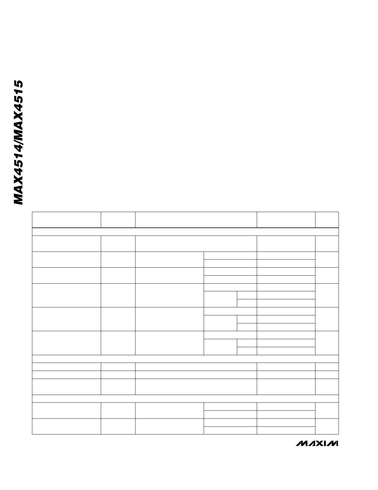
ELECTRICAL CHARACTERISTICS— +5V Supply
(V+ = +4.5V to +5.5V, VINH = 2.4V, VINL = 0.8V, TA = TMIN to TMAX, unless otherwise noted. Typical values are at TA = +25°C.)
PARAMETER
SYMBOL
CONDITIONS
MIN TYP MAX
(Note 2)
UNITS
ANALOG SWITCH
Analog Signal Range
VCOM, VNO,
VNC
0
V+
V
COM to NO or NC
On-Resistance
RON
V+ = 5V, VCOM = 3.5V,
ICOM = 1mA
TA = +25°C
TA = TMIN to TMAX
10 20
Ω
25
COM to NO or NC
On-Resistance Flatness
∆RON
VCOM = 1V, 2V, 3V;
ICOM = 1mA
TA = +25°C
TA = TMIN to TMAX
1
3
Ω
5
NO or NC Off-Leakage
Current (Note 3)
INO(OFF)
INC(OFF)
V+ = 5.5V,
VCOM = 1V,
VNO or VNC = 4.5V
TA = +25°C
-1 0.01 1
TA = TMIN
to TMAX
C, E
M
-20
-100
20
nA
100
COM Off-Leakage Current
(Note 3)
ICOM(OFF)
V+ = 5.5V,
VCOM = 4.5V,
VNO or VNC = 1V
TA = +25°C
-1 0.01 1
TA = TMIN
to TMAX
C, E
M
-20
-100
20
nA
100
COM On-Leakage Current
(Note 3)
ICOM(ON)
V+ = 5.5V,
VCOM = 4.5V,
VNO or VNC = 4.5V
TA = +25°C
-2 0.01 2
TA = TMIN
to TMAX
C, E
M
-40
-200
40
nA
200
DIGITAL I/O
Input Logic High
VIH
2.4
V+
V
Input Logic Low
VIL
0
0.8
V
Input Current Logic High
or Low
IIH, IIL
VIN = V+, 0V
-1 0.03 1
µA
SWITCH DYNAMIC CHARACTERISTICS
Turn-On Time
Turn-Off Time
tON
Figure 2
tOFF
Figure 2
TA = +25°C
TA = TMIN to TMAX
TA = +25°C
TA = TMIN to TMAX
30 150
ns
240
20 100
ns
150
2 _______________________________________________________________________________________
Share Link: 